

Complete Report - University of New South Wales
Complete Report - University of New South Wales
Complete Report - University of New South Wales
- No tags were found...

You also want an ePaper? Increase the reach of your titles
YUMPU automatically turns print PDFs into web optimized ePapers that Google loves.
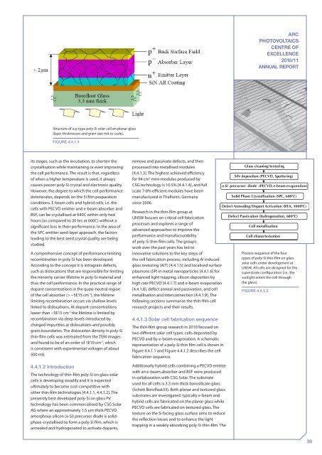
ARCPHOTOVOLTAICSCENTRE OFEXCELLENCE2010/11ANNUAL REPORTStructure <strong>of</strong> a p-type poly-Si solar cell on planar glass(layer thicknesses and grain size not to scale).Figure 4.4.1.1its stages, such as the incubation, to shorten thecrystallisation while maintaining or even improvingthe cell performance. The result is that, regardless<strong>of</strong> when a higher temperature is used, it alwayscauses poorer poly-Si crystal and electronic quality.However, the degree to which the cell performancedeteriorates, depends on the Si film preparationconditions. E-beam cells and hybrid cells, i.e. thecells with PECVD emitter and e-beam absorber andBSF, can be crystallised at 640C within only twohours (as compared to 20 hrs at 600C) without asignificant loss in their performance. In the area <strong>of</strong>the SPC emitter seed-layer approach, the factorsleading to the best seed crystal quality are beingstudied.A comprehensive concept <strong>of</strong> performance limitingrecombination in poly-Si has been developed.According to the concept it is intragrain defects,such as dislocations that are responsible for limitingthe minority carrier lifetime in poly-Si material andthus the cell performance. In the practical range <strong>of</strong>dopant concentrations in the quasi-neutral region<strong>of</strong> the cell absorber (> ~5E15 cm -3 ), the lifetimelimiting recombination occurs via shallow levelslinked to dislocations. At dopant concentrationslower than ~5E15 cm -3 the lifetime is limited byrecombination via deep levels introduced bycharged impurities at dislocations and possiblygrain-boundaries. The dislocation density in poly-Sithin-film cells was estimated from the TEM imagesand found to be <strong>of</strong> an order <strong>of</strong> 1E10 cm -2 , whichis consistent with experimental voltages <strong>of</strong> about500 mV.4.4.1.2 IntroductionThe technology <strong>of</strong> thin-film poly-Si on glass solarcells is developing steadily and it is expectedultimately to become cost-competitive withother thin-film technologies [4.4.1.1, 4.4.1.2]. Thepresently best developed poly-Si on glass PVtechnology has been commercialised by CSG SolarAG where an approximately 1.5 mm thick PECVDamorphous silicon (a-Si) precursor diode is solidphase-crystallisedto form a poly-Si film, which isannealed and hydrogenated to activate dopants,remove and passivate defects, and thenprocessed into metallised modules[4.4.1.3]. The highest achieved efficiencyfor 94 cm 2 mini-modules produced byCSG technology is 10.5% [4.4.1.4], and fullscale 7-8% efficient modules have beenmanufactured in Thalheim, Germanysince 2006.Research in the thin-film group atUNSW focuses on critical cell fabricationprocesses and explores a range <strong>of</strong>advanced approaches to improve theperformance and manufacturability<strong>of</strong> poly-Si thin-film cells. The group’swork over the past years has led toinnovative solutions to the key steps <strong>of</strong>the cell fabrication process, including Al inducedglass texturing (AIT) [4.4.1.5] and localised surfaceplasmons (SP) in metal nanoparticles [4.4.1.6] forenhanced light trapping, silicon deposition byhigh rate PECVD [4.4.1.7] and e-beam evaporation[4.4.1.8], defect anneal and passivation, and cellmetallisation and interconnection [4.4.1.9]. Thefollowing sections summarise the thin-film cellresearch projects and their results.4.4.1.3 Solar cell fabrication sequenceThe thin-film group research in 2010 focused ontwo different solar cell types: cells deposited byPECVD and by e-beam evaporation. A schematicrepresentation <strong>of</strong> a poly-Si thin film cell is shown inFigure 4.4.1.1 and Figure 4.4.1.2 describes the cellfabrication sequence.Additionally hybrid cells combining a PECVD emitterwith an e-beam absorber and BSF were producedin collaboration with CSG Solar. The substrateused for all cells is 3.3 mm thick borosilicate glass(Schott Bor<strong>of</strong>loat33). Both planar and textured glasssubstrates are investigated: typically e-beam andhybrid cells are fabricated on the planar glass whilePECVD cells are fabricated on textured glass. Thetexture on the Si facing glass surface aims to reducethe reflection losses and to enhance the lighttrapping in a weakly absorbing poly-Si thin-film. TheProcess sequence <strong>of</strong> the fourtypes <strong>of</strong> poly-Si thin-film on glasssolar cells under development atUNSW. All cells are designed for thesuperstrate configuration (i.e., thesunlight enters the cell throughthe glass).Figure 4.4.1.239


