

Complete Report - University of New South Wales
Complete Report - University of New South Wales
Complete Report - University of New South Wales
- No tags were found...

You also want an ePaper? Increase the reach of your titles
YUMPU automatically turns print PDFs into web optimized ePapers that Google loves.
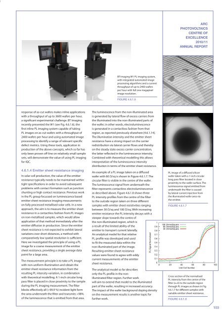
ARCPHOTOVOLTAICSCENTRE OFEXCELLENCE2010/11ANNUAL REPORTBT-Imaging W1 PL imaging system,with integrated automated imageprocessing algorithms and a currentthroughput <strong>of</strong> up to 2400 wafersper hour with full one megapixelimage resolution.Figure 4.6.1.6response <strong>of</strong> as-cut wafers makes inline applicationswith a throughput <strong>of</strong> up to 3600 wafers per hour,a significant experimental challenge. BT Imagingrecently presented the W1 (see Fig. 4.6.1.6), thefirst inline PL imaging system capable <strong>of</strong> takingPL images on as-cut wafers with a throughput <strong>of</strong>2400 wafers per hour and using automated imageprocessing to identify a range <strong>of</strong> relevant specificdefect metrics. Using these tools, application inproduction <strong>of</strong> the above concepts, which so far hasonly been proven <strong>of</strong>f-line on relatively small samplesets, will demonstrate the value <strong>of</strong> using PL imagingfor IQC.4.6.1.4 Emitter sheet resistance imagingIn solar cell production, the value <strong>of</strong> the emitterresistance typically needs to be maintained withintight specifications in order to avoid subsequentproblems with contact formation such as junctionshunting or high contact resistance. Previous workin the PL group focussed on luminescence basedemitter sheet resistance imaging measurementson fully processed metallised solar cells. In a newapproach, the aim is to measure the emitter sheetresistance in a contactless fashion from PL imageson non-metallised samples, which would allowapplication <strong>of</strong> that method immediately after theemitter diffusion in production. Since the emittersheet resistance is not expected to exhibit lateralvariations over short distances, a method withcomparatively low spatial resolution is sufficient.Here we investigated the principle <strong>of</strong> using a PLimage for a coarse measurement <strong>of</strong> the emittersheet resistance, providing a single average datapoint for a large area.The measurement principle is to take a PL imagewith non-uniform illumination and obtain theemitter sheet resistance information from theresulting PL intensity variation, in combinationwith theoretical modelling. A 1-inch circular longpass filter is placed in close proximity to the sampleduring the PL imaging measurement. The filterblocks effectively all (>99.9 %) incident light formthe area underneath the filter and transmits >98%<strong>of</strong> the luminescence that is emitted from that area.The luminescence from the non-illuminated areais generated by lateral flow <strong>of</strong> excess carriers fromthe illuminated into the non-illuminated parts <strong>of</strong>the wafer, in other words, electroluminescenceis generated in a contactless fashion from thatregion, as reported previously elsewhere [4.6.1.14].The illumination intensity and the emitter sheetresistance have a strong impact on the carrierredistribution via lateral carrier flows and therebyon the steady state excess carrier concentration,the latter reflected in the luminescence intensity.Combined with theoretical modelling this allowsinterpretation <strong>of</strong> the luminescence intensitydistribution in terms <strong>of</strong> the emitter sheet resistance.An example <strong>of</strong> a PL image taken on a diffusedwafer with 60 Ω/sq is shown in Figure 4.6.1.7. Thecircular filter is visible in the centre <strong>of</strong> the wafer.The luminescence signal from underneath thefilter represents contactless electroluminescenceas described above. Figure 4.6.1.8 shows threePL intensity pr<strong>of</strong>iles from the centre <strong>of</strong> the filterto the outside region taken on three differentsamples with emitter sheet resistivities rangingbetween 30 Ω/sq and 100 Ω/sq. With increasingemitter resistance the PL intensity decays with asteeper slope towards the centre <strong>of</strong>the non-illuminated region, which isa result <strong>of</strong> the limited ability <strong>of</strong> theemitter to transport current laterally.An analytical model for that relativePL pr<strong>of</strong>ile was developed and usedto fit the measured data within thenon-illuminated part <strong>of</strong> the image.Resulting emitter sheet resistancevalues were found to agree with eddycurrent measurements <strong>of</strong> the emittersheet resistance.The analytical model so far describesonly the PL pr<strong>of</strong>ile in the nonilluminatedfilter region. Further workwill aim to extend that model to the illuminatedpart <strong>of</strong> the wafer, resulting in increased accuracy.The impact <strong>of</strong> the wafer background doping densityon the measurement results is another topic forfurther work.PL image <strong>of</strong> a diffused siliconwafer taken with a 1-inch circularlong pass filter located in closeproximity to the wafer surface. Theluminescence signal emitted fromunderneath the filter is causedby lateral current injection fromthe illuminated wafer area viathe emitter.Figure 4.6.1.7Cross section <strong>of</strong> the normalisedPL intensity from the centre <strong>of</strong> thefilter (x=0) to the outside regionthrough PL images as shown in Fig4.6.1.7 for different samples withvariable emitter sheet resistance.Figure 4.6.1.8103


