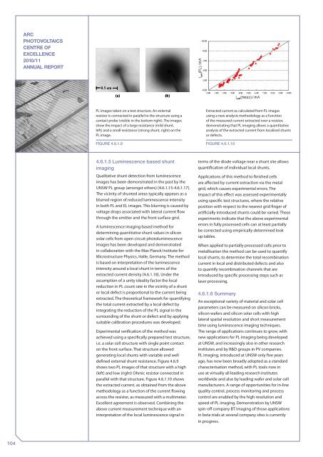
ARCPHOTOVOLTAICSCENTRE OFEXCELLENCE2010/11ANNUAL REPORT0.5 cm(a)(b)PL images taken on a test structure. An externalresistor is connected in parallel to the structure using acontact probe (visible in the bottom right). The imagesshow the impact <strong>of</strong> a large resistance (mild shunt,left) and a small resistance (strong shunt, right) on thePL image.Figure 4.6.1.9Extracted current as calculated from PL imagesusing a new analysis methodology as a function<strong>of</strong> the measured current extracted over a resistor,demonstrating that PL imaging allows a quantitativeanalysis <strong>of</strong> the extracted current from localised shuntsor defects.Figure 4.6.1.104.6.1.5 Luminescence based shuntimagingQualitative shunt detection from luminescenceimages has been demonstrated in the past by theUNSW PL group (amongst others) [4.6.1.15-4.6.1.17].The vicinity <strong>of</strong> shunted areas typically appears as ablurred region <strong>of</strong> reduced luminescence intensityin both PL and EL images. This blurring is caused byvoltage drops associated with lateral current flowthrough the emitter and the front surface grid.A luminescence imaging based method fordetermining quantitative shunt values in siliconsolar cells from open circuit photoluminescenceimages has been developed and demonstratedin collaboration with the Max Planck Institute forMicrostructure Physics, Halle, Germany. The methodis based on interpretation <strong>of</strong> the luminescenceintensity around a local shunt in terms <strong>of</strong> theextracted current density [4.6.1.18]. Under theassumption <strong>of</strong> a unity ideality factor the localreduction in PL count rate in the vicinity <strong>of</strong> a shuntor local defect is proportional to the current beingextracted. The theoretical framework for quantifyingthe total current extracted by a local defect byintegrating the reduction <strong>of</strong> the PL signal in thesurrounding <strong>of</strong> the shunt or defect and by applyingsuitable calibration procedures was developed.Experimental verification <strong>of</strong> the method wasachieved using a specifically prepared test structure,i.e. a solar cell structure with single point contacton the front surface. That structure allowedgenerating local shunts with variable and welldefined external shunt resistance. Figure 4.6.9shows two PL images <strong>of</strong> that structure with a high(left) and low (right) Ohmic resistor connected inparallel with that structure. Figure 4.6.1.10 showsthe extracted current, as obtained from the abovemethodology as a function <strong>of</strong> the current flowingacross the resistor, as measured with a multimeter.Excellent agreement is observed. Combining theabove current measurement technique with aninterpretation <strong>of</strong> the local luminescence signal interms <strong>of</strong> the diode voltage near a shunt site allowsquantification <strong>of</strong> individual local shunts.Applications <strong>of</strong> this method to finished cellsare affected by current extraction via the metalgrid, which causes experimental errors. Theimpact <strong>of</strong> this effect was assessed experimentallyusing specific test structures, where the relativeposition with respect to the nearest grid finger <strong>of</strong>artificially introduced shunts could be varied. Theseexperiments indicate that the above experimentalerrors in fully processed cells can at least partiallybe corrected using empirically determined lookup tables.When applied to partially processed cells prior tometallisation the method can be used to quantifylocal shunts, to determine the total recombinationcurrent in local and distributed defects and alsoto quantify recombination channels that areintroduced by specific processing steps such aslaser processing.4.6.1.6 SummaryAn exceptional variety <strong>of</strong> material and solar cellparameters can be measured on silicon bricks,silicon wafers and silicon solar cells with highlateral spatial resolution and short measurementtime using luminescence imaging techniques.The range <strong>of</strong> applications continues to grow, withnew applications for PL imaging being developedat UNSW, and increasingly also in other researchinstitutes and by R&D groups in PV companies.PL imaging, introduced at UNSW only five yearsago, has now been broadly adopted as a standardcharacterisation method, with PL tools now inuse at virtually all leading research institutesworldwide and also by leading wafer and solar cellmanufacturers. A range <strong>of</strong> opportunities for in-linequality control, process monitoring and processcontrol are enabled by the high resolution andspeed <strong>of</strong> PL imaging. Demonstration by UNSWspin-<strong>of</strong>f company BT Imaging <strong>of</strong> those applicationsin beta trials at several company sites is currentlyin progress.104
References4.6.1.1 McMillan, W. et al., In-line monitoring <strong>of</strong> electricalwafer quality using photoluminescence imaging.Proceedings <strong>of</strong> 25th EPVSC, Valencia, Spain,September, 2010.4.6.1.2 Trupke, T., Nyhus, J. and Haunschild, J.,Luminescence imaging for inline characterisation insilicon photovoltaics. Phys.Stat.Solidi RRL, 2011: p.published online February 2011.4.6.1.3 Fuyuki, T. et al., One shot mapping <strong>of</strong> minoritycarrier diffusion lenth in polycrystalline Si solar cellsusing electroluminescence. 31st IEEE PhotovoltaicSpecialists Conference, Orlando, USA, 2005.4.6.1.4 Trupke, T. et al., Fast photoluminescence imaging <strong>of</strong>silicon wafers. WCPEC-4, Waikoloa, USA, 2006.4.6.1.5 Trupke, T., et al., Spatially resolved series resistance<strong>of</strong> silicon solar cells obtained from luminescenceimaging. Appl. Phys. Lett., 2007. 90: p. 093506.4.6.1.6 Kampwerth, H. et al., Advanced luminescence basedeffective series resistance imaging <strong>of</strong> silicon solarcells. Appl. Phys. Lett., 2008. 93: p. 202102.4.6.1.7 Haunschild, J. et al., Quality control <strong>of</strong> ascutmulticrystalline silicon wafers usingphotoluminescene imaging for solar cell production.Solar Energy Materials and Solar Cells, 2010.94(12): p. 2007-2012.4.6.1.8 You, D. et al., The dislocation distributioncharacterisitics <strong>of</strong> multi-crystalline silicon ingotand its impact on cell efficiency. 35th IEEE PVSC,Honululu, USA, June, 2010.4.6.1.9 Trupke, T., Bardos, R.A. and Nyhus, J.,Photoluminescence characterisation <strong>of</strong> silicon wafersand solar cells. 18th workshop on Crystalline SiliconSolar cells & Modules, 2008.4.6.1.10 Trupke, T. et al., Bulk minority carrier lifeitmefrom luminescence intensity ratios measuredon silicon bricks. 25th EPVSC, Valencia, Spain,September 2010.4.6.1.11 Mitchell, B. et al., Bulk minority carrier lifetimes anddoping <strong>of</strong> silicon bricks from photoluminescenceintensity ratios. J. Appl.Phys., 2011: p. acceptedfor publication.4.6.1.12 Würfel, P. et al., Diffusion lengths <strong>of</strong> silicon solarcells obtained from luminescence images. Journal <strong>of</strong>Applied Physics, 2007. 101: p. 123110.4.6.1.13 Demant, M. et al., Analysis <strong>of</strong> luminescenceimages applying pattern recoginition techniques.Proceedings <strong>of</strong> 25th EPVSC, Valencia, Spain,September, 2010.4.6.1.14 Sinton, R.A., Contactless electroluminescence forshunt-value measurement in solar cells. Proceedings<strong>of</strong> the 23rd EPVSC, Valencia, September, 2008:p. 1157.4.6.1.15 Trupke, T. et al., Luminescence imaging for fastshunt localisation in silicon solar cells and siliconwafers. International Workshop on Science andTechnology <strong>of</strong> Crystalline Silicon Solar Cells,Sendai, Japan, 2-3 October, 2006.4.6.1.16 Kasemann, M. et al., Shunt detection capabilities <strong>of</strong>luminescence imaging on silicon solar cells. 22ndEuropean Photovoltaic Solar Energy Conference,Milan, Italy, 2007.4.6.1.17 Breitenstein, O. et al., On the detection <strong>of</strong> shunts insilicon solar cells by photo- and electroluminescenceimaging progress in Photovoltaics, 2008. 16: p. 325.4.6.1.18 Augarten, Y. et al., Luminescence shunt imaging:qualitative and quantitative shunt images usingphotoluminesccence imaging. 24th EuropeanPhotovoltaic Solar Energy Conference, Hamburg,September, 2009.4.6.2 General Characterisation<strong>University</strong> StaffDr Henner KampwerthProject Scientists and TechniciansAlan YeeThe range <strong>of</strong> research undertaken by the Centreinvolves a variety <strong>of</strong> measurement techniquesfor the characterisation <strong>of</strong> photovoltaic materialsand devices. Understanding and utilising thesetechniques appropriately, and improving themwhere possible, is crucial in order to maintain theworld-class reputation <strong>of</strong> our research output.Improvements to measurement techniques with thegoal <strong>of</strong> producing more accurate and meaningfulresults will have a direct impact both on researchactivities and on the optimization <strong>of</strong> proceduresused in manufacturing. The time and number<strong>of</strong> experiments needed to understand a certainphenomena can be greatly reduced. The need tomeasure parameters <strong>of</strong> interest more precisely,without the possibility <strong>of</strong> misinterpretation, istherefore high. The General Characterisation groupwas formed in July 2010 to address this need.The group primarily focuses on opticalcharacterization methods such asphotoluminescence spectroscopy and absorptionspectroscopy. In recent years, it has been shownthat these optical measurements can be used toextract a large number <strong>of</strong> material and deviceproperties. In addition the ability to performcontactless non-destructive probing <strong>of</strong> small areasdown to a few ten micrometers in diameter makesoptical measurement techniques very attractive forsamples that cannot be measured otherwise.In addition, the group will review somecommonly used measurement methods withthe aim <strong>of</strong> automating parameter extractionfrom measurement data. It is common that lessexperienced researchers misinterpret data and drawincorrect conclusions. Computer programs thatassist in various levels <strong>of</strong> interpretation thereforecan prove their value. Some computer programswritten in the course <strong>of</strong> this work will be madeavailable for public use.ARCPHOTOVOLTAICSCENTRE OFEXCELLENCE2010/11ANNUAL REPORT105