

Complete Report - University of New South Wales
Complete Report - University of New South Wales
Complete Report - University of New South Wales
- No tags were found...

Create successful ePaper yourself
Turn your PDF publications into a flip-book with our unique Google optimized e-Paper software.
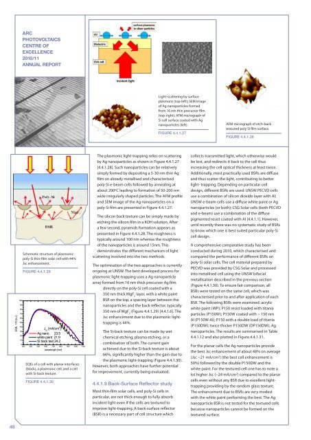
ARCPHOTOVOLTAICSCENTRE OFEXCELLENCE2010/11ANNUAL REPORTLight-scattering by surfaceplasmons (top-left); SEM image<strong>of</strong> Ag nanoparticles formedfrom 16 nm thin precursor film(top-right); AFM micrograph <strong>of</strong>Si cell surface coated with Agnanoparticles (left).Figure 4.4.1.27AFM micrograph <strong>of</strong> etch-backtextured poly Si film surface.Figure 4.4.1.28EQE, 1-R [a.u.]100908070605040302010Schematic structure <strong>of</strong> plasmonicpoly-Si thin-film solar cell with 44%Jsc enhancement.Figure 4.4.1.29J sc[mA/cm 2 ]Ag nano 23.5white paint 21.9Si back text 24.20300 400 500 600 700 800 900 1000 1100wavelength [nm]EQEs <strong>of</strong> a cell with planar interfaces(black), a plasmonic cell, and a cellwith Si-back texture.Figure 4.4.1.30The plasmonic light-trapping relies on scatteringby Ag nanoparticles as shown in Figure 4.4.1.27[4.4.1.28]. Such nanoparticles can be relativelysimply formed by depositing a 5-30 nm thin Agfilm on already metallised and characterisedpoly-Si e-beam cells followed by annealing atabout 200ºC leading to formation <strong>of</strong> 50-200 nmwide irregularly shaped particles. The AFM pr<strong>of</strong>ileand SEM image <strong>of</strong> the Ag nanoparticles on apoly-Si film are presented in Figure 4.4.1.27.The silicon back texture can be simply made byetching the silicon film in a KOH solution. Aftera few second, pyramids formation appears aspresented in Figure 4.4.1.28. The roughness istypically around 100 nm whereas the roughness<strong>of</strong> the nanoparticles is around 15nm. Thisdemonstrates the different mechanism <strong>of</strong> lightscattering involved into the two methods.The optimisation <strong>of</strong> the two approaches is currentlyongoing at UNSW. The best developed process forplasmonic light-trapping uses a Ag nanoparticlearray formed from 16 nm thick precursor Ag filmdirectly on the poly-Si cell coated with a350 nm thick MgF 2layer, with a white paintBSR on the top, a spacing layer between thenanoparticles and the back reflector, typically350 nm <strong>of</strong> MgF 2(Figure 4.4.1.29) [4.4.1.6]. TheJsc enhancement due to the plasmonic lighttrappingis 44%.The Si-back texture can be made by wetchemical etching, plasma etching, or acombination <strong>of</strong> both. The current gainachieved due to the Si-back texture is about66%, significantly higher than the gain due tothe plasmonic light-trapping (Figure 4.4.1.30).However, both approaches have further potentialfor improvement, currently being evaluated.4.4.1.9 Back-Surface Reflector studyMost thin-film solar cells, and poly-Si cells inparticular, are not thick enough to fully absorbincident light even if the cells are textured toimprove light-trapping. A back-surface reflector(BSR) is a necessary part <strong>of</strong> cell structure whichcollects transmitted light, which otherwise wouldbe lost, and redirects it back to the cell thusincreasing the cell optical thickness at least twice.Additionally, most practically used BSRs are diffuseand thus scatter the light, contributing to betterlight- trapping. Depending on particular celldesign, different BSRs are used: UNSW PECVD cellsuse a combination <strong>of</strong> silicon dioxide layer with Al;UNSW e-beam cells use a diffuse white paint or Agnanoparticles (or both); CSG Solar cells (both PECVDand e-beam) use a combination <strong>of</strong> the diffusepigmented resist coated with Al [4.4.1.1]. However,until recently there was no systematic study <strong>of</strong> BSRsto know which one is best suited particular poly-Sicell design.A comprehensive comparative study has beenconducted during 2010, which characterised andcompared the performance <strong>of</strong> different BSRs onpoly-Si solar cells. The cell material prepared byPECVD was provided by CSG Solar and processedinto metallised cell using the UNSW bifacialmetallisation described in the previous section(Figure 4.4.1.30). To ensure fair comparison, allBSRs were tested on the same cell, which wascharacterised prior to and after application <strong>of</strong> eachBSR. The following BSRs were examined: acrylicwhite paint (WP); P150 resist loaded with titaniaparticles (P150W); P150W coated with ~ 150 nmAl (P150W-Al); P150 with a double load <strong>of</strong> titania(P150DW); twice thicker P150DW (DP150DW); Agnanoparticles. The results are summarised in Table4.4.1.12 and also plotted in Figure 4.4.1.31.For the planar cells the Ag nanoparticles providethe best Jsc enhancement <strong>of</strong> about 48% on average(Jsc ~21 mA/cm 2 ) (the best cell enhancement is50%) followed by the double P150DW and thewhite paint. For the textured cell one has to note alot higher Jsc (~24 mA/cm 2 ) compared to the planarcells even without any BSR due to excellent lighttrappingproviding by the random glass texture.The enhancement due to BSRs are very modestwith the white paint performing the best. The Agnanoparticle BSR is not tested for the textured cellsbecause nanoparticles cannot be formed on thetextured surface.48


