

Complete Report - University of New South Wales
Complete Report - University of New South Wales
Complete Report - University of New South Wales
- No tags were found...

Create successful ePaper yourself
Turn your PDF publications into a flip-book with our unique Google optimized e-Paper software.
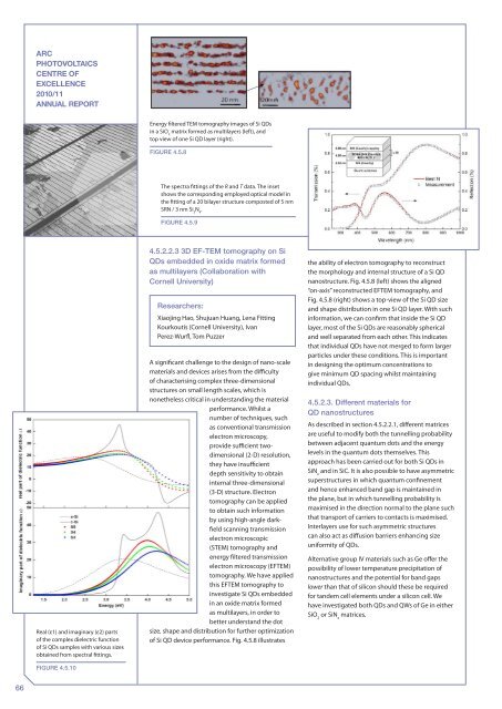
ARCPHOTOVOLTAICSCENTRE OFEXCELLENCE2010/11ANNUAL REPORTEnergy filtered TEM tomography images <strong>of</strong> Si QDsin a SiO 2matrix formed as multilayers (left), andtop view <strong>of</strong> one Si QD layer (right).Figure 4.5.8The spectra fittings <strong>of</strong> the R and T data. The insetshows the corresponding employed optical model inthe fitting <strong>of</strong> a 20 bilayer structure composted <strong>of</strong> 5 nmSRN / 3 nm Si 3N 4.Figure 4.5.9Real (ε1) and imaginary (ε2) parts<strong>of</strong> the complex dielectric function<strong>of</strong> Si QDs samples with various sizesobtained from spectral fittings.Figure 4.5.104.5.2.2.3 3D EF-TEM tomography on SiQDs embedded in oxide matrix formedas multilayers (Collaboration withCornell <strong>University</strong>)Researchers:Xiaojing Hao, Shujuan Huang, Lena FittingKourkoutis (Cornell <strong>University</strong>), IvanPerez‐Wurfl, Tom PuzzerA significant challenge to the design <strong>of</strong> nano-scalematerials and devices arises from the difficulty<strong>of</strong> characterising complex three-dimensionalstructures on small length scales, which isnonetheless critical in understanding the materialperformance. Whilst anumber <strong>of</strong> techniques, suchas conventional transmissionelectron microscopy,provide sufficient twodimensional(2-D) resolution,they have insufficientdepth sensitivity to obtaininternal three-dimensional(3-D) structure. Electrontomography can be appliedto obtain such informationby using high-angle darkfieldscanning transmissionelectron microscopic(STEM) tomography andenergy filtered transmissionelectron microscopy (EFTEM)tomography. We have appliedthis EFTEM tomography toinvestigate Si QDs embeddedin an oxide matrix formedas multilayers, in order tobetter understand the dotsize, shape and distribution for further optimization<strong>of</strong> Si QD device performance. Fig. 4.5.8 illustratesthe ability <strong>of</strong> electron tomography to reconstructthe morphology and internal structure <strong>of</strong> a Si QDnanostructure. Fig. 4.5.8 (left) shows the aligned“on-axis” reconstructed EFTEM tomography, andFig. 4.5.8 (right) shows a top-view <strong>of</strong> the Si QD sizeand shape distribution in one Si QD layer. With suchinformation, we can confirm that inside the Si QDlayer, most <strong>of</strong> the Si QDs are reasonably sphericaland well separated from each other. This indicatesthat individual QDs have not merged to form largerparticles under these conditions. This is importantin designing the optimum concentrations togive minimum QD spacing whilst maintainingindividual QDs.4.5.2.3. Different materials forQD nanostructuresAs described in section 4.5.2.2.1, different matricesare useful to modify both the tunnelling probabilitybetween adjacent quantum dots and the energylevels in the quantum dots themselves. Thisapproach has been carried out for both Si QDs inSiN xand in SiC. It is also possible to have asymmetricsuperstructures in which quantum confinementand hence enhanced band gap is maintained inthe plane, but in which tunnelling probability ismaximised in the direction normal to the plane suchthat transport <strong>of</strong> carriers to contacts is maximised.Interlayers use for such asymmetric structurescan also act as diffusion barriers enhancing sizeuniformity <strong>of</strong> QDs.Alternative group IV materials such as Ge <strong>of</strong>fer thepossibility <strong>of</strong> lower temperature precipitation <strong>of</strong>nanostructures and the potential for band gapslower than that <strong>of</strong> silicon should these be requiredfor tandem cell elements under a silicon cell. Wehave investigated both QDs and QWs <strong>of</strong> Ge in eitherSiO 2or SiN xmatrices.66


