

Complete Report - University of New South Wales
Complete Report - University of New South Wales
Complete Report - University of New South Wales
- No tags were found...

You also want an ePaper? Increase the reach of your titles
YUMPU automatically turns print PDFs into web optimized ePapers that Google loves.
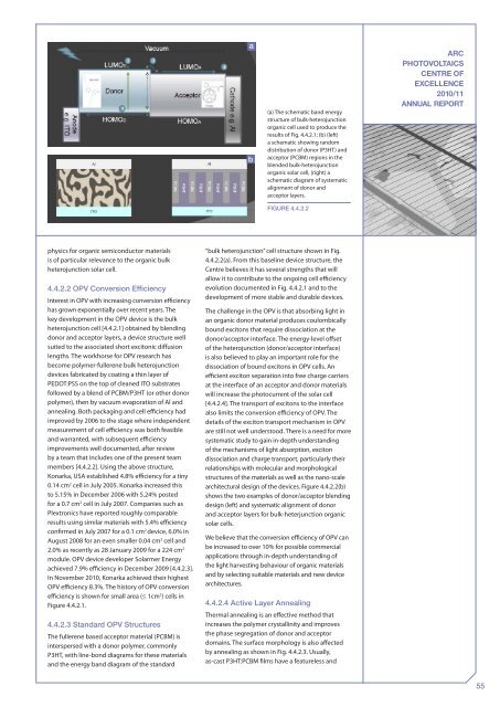
(a) The schematic band energystructure <strong>of</strong> bulk-heterojunctionorganic cell used to produce theresults <strong>of</strong> Fig. 4.4.2.1; (b) (left)a schematic showing randomdistribution <strong>of</strong> donor (P3HT) andacceptor (PCBM) regions in theblended bulk-heterojunctionorganic solar cell, (right) aschematic diagram <strong>of</strong> systematicalignment <strong>of</strong> donor andacceptor layers.ARCPHOTOVOLTAICSCENTRE OFEXCELLENCE2010/11ANNUAL REPORTFigure 4.4.2.2physics for organic semiconductor materialsis <strong>of</strong> particular relevance to the organic bulkheterojunction solar cell.4.4.2.2 OPV Conversion EfficiencyInterest in OPV with increasing conversion efficiencyhas grown exponentially over recent years. Thekey development in the OPV device is the bulkheterojunction cell [4.4.2.1] obtained by blendingdonor and acceptor layers, a device structure wellsuited to the associated short excitonic diffusionlengths. The workhorse for OPV research hasbecome polymer-fullerene bulk heterojunctiondevices fabricated by coating a thin layer <strong>of</strong>PEDOT:PSS on the top <strong>of</strong> cleaned ITO substratesfollowed by a blend <strong>of</strong> PCBM/P3HT (or other donorpolymer), then by vacuum evaporation <strong>of</strong> Al andannealing. Both packaging and cell efficiency hadimproved by 2006 to the stage where independentmeasurement <strong>of</strong> cell efficiency was both feasibleand warranted, with subsequent efficiencyimprovements well documented, after reviewby a team that includes one <strong>of</strong> the present teammembers [4.4.2.2]. Using the above structure,Konarka, USA established 4.8% efficiency for a tiny0.14 cm 2 cell in July 2005. Konarka increased thisto 5.15% in December 2006 with 5.24% postedfor a 0.7 cm 2 cell in July 2007. Companies such asPlextronics have reported roughly comparableresults using similar materials with 5.4% efficiencyconfirmed in July 2007 for a 0.1 cm 2 device, 6.0% inAugust 2008 for an even smaller 0.04 cm 2 cell and2.0% as recently as 28 January 2009 for a 224 cm 2module. OPV device developer Solarmer Energyachieved 7.9% efficiency in December 2009 [4.4.2.3].In November 2010, Konarka achieved their highestOPV efficiency 8.3%. The history <strong>of</strong> OPV conversionefficiency is shown for small area (≤ 1cm 2 ) cells inFigure 4.4.2.1.4.4.2.3 Standard OPV StructuresThe fullerene based acceptor material (PCBM) isinterspersed with a donor polymer, commonlyP3HT, with line-bond diagrams for these materialsand the energy band diagram <strong>of</strong> the standard“bulk heterojunction” cell structure shown in Fig.4.4.2.2(a). From this baseline device structure, theCentre believes it has several strengths that willallow it to contribute to the ongoing cell efficiencyevolution documented in Fig. 4.4.2.1 and to thedevelopment <strong>of</strong> more stable and durable devices.The challenge in the OPV is that absorbing light inan organic donor material produces coulombicallybound excitons that require dissociation at thedonor/acceptor interface. The energy-level <strong>of</strong>fset<strong>of</strong> the heterojunction (donor/acceptor interface)is also believed to play an important role for thedissociation <strong>of</strong> bound excitons in OPV cells. Anefficient exciton separation into free charge carriersat the interface <strong>of</strong> an acceptor and donor materialswill increase the photocurrent <strong>of</strong> the solar cell[4.4.2.4]. The transport <strong>of</strong> excitons to the interfacealso limits the conversion efficiency <strong>of</strong> OPV. Thedetails <strong>of</strong> the exciton transport mechanism in OPVare still not well understood. There is a need for moresystematic study to gain in-depth understanding<strong>of</strong> the mechanisms <strong>of</strong> light absorption, excitondissociation and charge transport, particularly theirrelationships with molecular and morphologicalstructures <strong>of</strong> the materials as well as the nano-scalearchitectural design <strong>of</strong> the devices. Figure 4.4.2.2(b)shows the two examples <strong>of</strong> donor/acceptor blendingdesign (left) and systematic alignment <strong>of</strong> donorand acceptor layers for bulk-heterjunction organicsolar cells.We believe that the conversion efficiency <strong>of</strong> OPV canbe increased to over 10% for possible commercialapplications through in-depth understanding <strong>of</strong>the light harvesting behaviour <strong>of</strong> organic materialsand by selecting suitable materials and new devicearchitectures.4.4.2.4 Active Layer AnnealingThermal annealing is an effective method thatincreases the polymer crystallinity and improvesthe phase segregation <strong>of</strong> donor and acceptordomains. The surface morphology is also affectedby annealing as shown in Fig. 4.4.2.3. Usually,as-cast P3HT:PCBM films have a featureless and55


