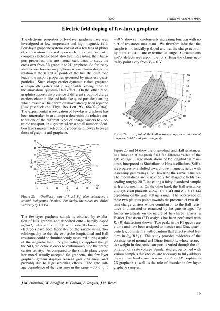
2009 CARBON ALLOTROPESElectric field doping of few-layer graph<strong>en</strong>eThe electronic properties of few-layer graph<strong>en</strong>e have be<strong>en</strong>investigated at low temperature and high magnetic field.Few-layer graph<strong>en</strong>e systems consist of a few t<strong>en</strong>s of planesof carbon atoms stacked upon each others and exhibit acomplex electronic band structure. Regarding their transportproperties, they are natural candidates to study thecross over from 3D graphite to 2D graph<strong>en</strong>e. So far, manystudies have focused on graph<strong>en</strong>e, where a linear dispersionrelation at the K and K ′ points of the first Brillouin zoneleads to transport properties governed by massless quasiparticles.Such charge carrier dynamic makes graph<strong>en</strong>ea unique 2D system and is responsible, among other, tothe anomalous quantum Hall effect. On the other hand,graphite supports the pres<strong>en</strong>ce of differ<strong>en</strong>t groups of chargecarriers (electron-like and hole-like quasi-particles), amongwhich massless Dirac fermions have already be<strong>en</strong> reported[Luk’yanchuck et al. Phys. Rev. Lett., 93, 166402 (2004)].The experim<strong>en</strong>tal investigation of few-layer graph<strong>en</strong>e hasbe<strong>en</strong> undertak<strong>en</strong> in an attempt to determine the relative contributionsof the differ<strong>en</strong>t types of charge carriers to electronictransport, in a system where a small number of carbonlayers makes its electronic properties half-way betwe<strong>en</strong>those of graphite and graph<strong>en</strong>e.+70 V shows a monotonously increasing function with nohint of resistance maximum. We therefore infer that thesample is intrinsically p-doped and that the charge neutralitypoint is out of the experim<strong>en</strong>tal range. Contaminantsand/or defects are responsible for shifting the charge neutralitypoint away from V g = 0 V.Figure 24: 3D plot of the Hall resistance R xy as a function ofmagnetic field B and gate voltage V gFigure 23: Oscillatory part of R xx (B,V g ) after subtracting asmooth background function. For clarity, the curves are shiftedvertically by 1.5 kΩThe few-layer graph<strong>en</strong>e sample is obtained by exfoliationof bulk graphite and deposited onto a heavily dopedSi/SiO 2 substrate with 300 nm oxide thickness. Fourelectro<strong>des</strong> have be<strong>en</strong> fabricated on the sample using photolithographyso that the two-probe longitudinal and Hallresistance could be simultaneously measured during a pulseof the magnetic field. A gate voltage is applied thoughthe SiO 2 dielectric in order to continuously tune the chargecarrier d<strong>en</strong>sity. As compared to the simple plane capacitormodel usually accepted for graph<strong>en</strong>e, the few-layergraph<strong>en</strong>e system displays reduced gate effici<strong>en</strong>cy, mostprobably due to large scre<strong>en</strong>ing effects. The gate voltagedep<strong>en</strong>d<strong>en</strong>ce of the resistance in the range −70 < V g
CARBON ALLOTROPES 2009Low temperature magneto-transport in natural graphiteHistorically, graph<strong>en</strong>e forms the starting point for the Slonczewski,Weiss and McClure (SWM) band structure calculationsof graphite. In graphite, the Bernal stacked graph<strong>en</strong>elayers are weakly coupled with the form of the in-planedispersion dep<strong>en</strong>ding upon the mom<strong>en</strong>tum k z in the directionperp<strong>en</strong>dicular to the layers. The carriers occupy a regionalong the H − K − H edge of the hexagonal Brillouinzone. At the K point (k z = 0), the dispersion of the electronpocket is parabolic (massive fermions), while at the H point(k z = 0.5) the dispersion of the hole pocket is linear (masslessDirac fermions). A clear signature of Dirac fermionsat the H point of graphite has rec<strong>en</strong>tly be<strong>en</strong> reported usingfar-infrared magneto-absorption and ARPES measurem<strong>en</strong>ts.Such measurem<strong>en</strong>ts probe the very close vicinity ofthe H and K points where there is a maximum in the jointd<strong>en</strong>sity of states.Typical low temperature R xx versus magnetic field for naturalgraphite, is shown in Fig. 25(a). The quantum oscillations,superimposed on a large magneto-resistance background,can be better se<strong>en</strong> in the background removed data∆R xx plotted in Fig. 25(a-c). Quantum oscillations are observedfor both majority electrons and holes with orbitalquantum number up to almost N = 100. These oscillationsare fully consist<strong>en</strong>t with the pres<strong>en</strong>ce of majority electronand hole pockets within the three dim<strong>en</strong>sional SWM bandstructure calculations for graphite [Schneider et al. Phys.Rev. Lett. 102, 166403 (2009)]. At low magnetic fields,a perfect linear behavior in N(1/B) is observed for bothelectrons and holes. For high magnetic fields, clear deviationsfrom the linear behavior are observed for the electronfeatures (see Fig. 26(b-c)). This deviation from a periodicin 1/B behavior at high magnetic fields is due to theFermi level moving as the quantum limit is approachedin graphite. Clearly, the high field data should not beused to extract the phase of the oscillations. Instead weuse the complex Fourier transform ˆf (B) of the low magneticfield ∆R xx (1/B). The phase shift function K(ϕ,B) =Re[e −iϕ ˆf (B)] has maximum in the ϕ − B plane which canbe used to extract both the frequ<strong>en</strong>cy (B) and phase (ϕ) ofthe oscillations. K(ϕ,B) is plotted in Fig. 26(d-e) in theregions of the hole and electron features. From the maxima,the determined frequ<strong>en</strong>cy and phase are B fh = 4.51 T,ϕ h = −(0.56±0.1)π and B fe = 6.14 T, ϕ e = −(0.86±0.1)πfor the hole and electron features respectively.We therefore conclude that we have no evid<strong>en</strong>ce for theexist<strong>en</strong>ce of masseless Dirac fermions with a Berry phaseγ = 0. Transport measurem<strong>en</strong>ts are s<strong>en</strong>sitive to the d<strong>en</strong>sityof states at E F , which is modulated with increasing magneticfield, as the Landau bands cross the Fermi <strong>en</strong>ergy. Forholes, maxima in the d<strong>en</strong>sity of states correspond to Landaubands crossing E F for k z < 0.5, away from the H point,where the dispersion is no longer linear and a priori there isno reason to expect the carriers to behave as Dirac fermions.Figure 25: (a) Resistance R xx versus B measured at T = 10 mKfor natural graphite. (a-c) Background removed data ∆R xx showingquantum oscillations measured over differ<strong>en</strong>t magnetic fieldregions. The arrows indicate spin split electron and hole features.Figure 26: (a) Fourier transform of the low magnetic field∆R xx (1/B). (b-c) Orbital angular mom<strong>en</strong>tum quantum numberN, as a function of the reciprocal magnetic field positions of theelectron and hole features. (d) and (e) Contour plot of the phaseshift function K(ϕ,B) in the vicinity of the hole and electron features.Maxima in K(ϕ,B) determines the frequ<strong>en</strong>cy and phase ofthe oscillations.J. M. Schneider, M. Orlita, M. Potemski and D. K. Maude20
- Page 1 and 2: LABORATOIRE NATIONAL DES CHAMPS MAG
- Page 4 and 5: TABLE OF CONTENTSPreface 1Carbon Al
- Page 6 and 7: Coexistence of closed orbit and qua
- Page 8: 2009PrefaceDear Reader,You have bef
- Page 12 and 13: 2009 CARBON ALLOTROPESInvestigation
- Page 14 and 15: 2009 CARBON ALLOTROPESPropagative L
- Page 16 and 17: 2009 CARBON ALLOTROPESEdge fingerpr
- Page 18 and 19: 2009 CARBON ALLOTROPESObservation o
- Page 20 and 21: 2009 CARBON ALLOTROPESImproving gra
- Page 22 and 23: 2009 CARBON ALLOTROPESHow perfect c
- Page 24 and 25: 2009 CARBON ALLOTROPESTuning the el
- Page 28 and 29: 2009 CARBON ALLOTROPESMagnetotransp
- Page 30 and 31: 2009 CARBON ALLOTROPESGraphite from
- Page 32: 2009Two-Dimensional Electron Gas25
- Page 35 and 36: TWO-DIMENSIONAL ELECTRON GAS 2009Di
- Page 37 and 38: TWO-DIMENSIONAL ELECTRON GAS 2009Sp
- Page 39 and 40: TWO-DIMENSIONAL ELECTRON GAS 2009Cr
- Page 41 and 42: TWO-DIMENSIONAL ELECTRON GAS 2009Re
- Page 43 and 44: TWO-DIMENSIONAL ELECTRON GAS 2009In
- Page 45 and 46: TWO-DIMENSIONAL ELECTRON GAS 2009Ho
- Page 47 and 48: TWO-DIMENSIONAL ELECTRON GAS 2009Te
- Page 50 and 51: 2009 SEMICONDUCTORS AND NANOSTRUCTU
- Page 52 and 53: 2009 SEMICONDUCTORS AND NANOSTRUCTU
- Page 54 and 55: 2009 SEMICONDUCTORS AND NANOSTRUCTU
- Page 56 and 57: 2009 SEMICONDUCTORS AND NANOSTRUCTU
- Page 58 and 59: 2009 SEMICONDUCTORS AND NANOSTRUCTU
- Page 60: 2009Metals, Superconductors and Str
- Page 63 and 64: METALS, SUPERCONDUCTORS... 2009Anom
- Page 65 and 66: METALS, SUPERCONDUCTORS... 2009Magn
- Page 67 and 68: METALS, SUPERCONDUCTORS ... 2009Coe
- Page 69 and 70: METALS, SUPERCONDUCTORS ... 2009Fie
- Page 71 and 72: METALS, SUPERCONDUCTORS... 2009High
- Page 73 and 74: METALS, SUPERCONDUCTORS... 2009Angu
- Page 75 and 76: METALS, SUPERCONDUCTORS... 2009Magn
- Page 77 and 78:
METALS, SUPERCONDUCTORS... 2009Meta
- Page 79 and 80:
METALS, SUPERCONDUCTORS... 2009Temp
- Page 81 and 82:
METALS, SUPERCONDUCTORS... 200974
- Page 84 and 85:
2009 MAGNETIC SYSTEMSY b 3+ → Er
- Page 86 and 87:
2009 MAGNETIC SYSTEMSMagnetotranspo
- Page 88 and 89:
2009 MAGNETIC SYSTEMSHigh field tor
- Page 90 and 91:
2009 MAGNETIC SYSTEMSNuclear magnet
- Page 92 and 93:
2009 MAGNETIC SYSTEMSStructural ana
- Page 94 and 95:
2009 MAGNETIC SYSTEMSEnhancement ma
- Page 96 and 97:
2009 MAGNETIC SYSTEMSInvestigation
- Page 98 and 99:
2009 MAGNETIC SYSTEMSField-induced
- Page 100 and 101:
2009 MAGNETIC SYSTEMSMagnetic prope
- Page 102:
2009Biology, Chemistry and Soft Mat
- Page 105 and 106:
BIOLOGY, CHEMISTRY AND SOFT MATTER
- Page 108 and 109:
2009 APPLIED SUPERCONDUCTIVITYMagne
- Page 110 and 111:
2009 APPLIED SUPERCONDUCTIVITYPhtha
- Page 112:
2009Magneto-Science105
- Page 115 and 116:
MAGNETO-SCIENCE 2009Study of the in
- Page 117 and 118:
MAGNETO-SCIENCE 2009Magnetohydrodyn
- Page 119 and 120:
MAGNETO-SCIENCE 2009112
- Page 122 and 123:
2009 MAGNET DEVELOPMENT AND INSTRUM
- Page 124 and 125:
2009 MAGNET DEVELOPMENT AND INSTRUM
- Page 126 and 127:
2009 MAGNET DEVELOPMENT AND INSTRUM
- Page 128 and 129:
2009 MAGNET DEVELOPMENT AND INSTRUM
- Page 130 and 131:
2009 MAGNET DEVELOPMENT AND INSTRUM
- Page 132 and 133:
2009 MAGNET DEVELOPMENT AND INSTRUM
- Page 134 and 135:
2009 MAGNET DEVELOPMENT AND INSTRUM
- Page 136 and 137:
2009 PROPOSALSProposals for Magnet
- Page 138 and 139:
2009 PROPOSALSSpin-Jahn-Teller effe
- Page 140 and 141:
2009 PROPOSALSQuantum Oscillations
- Page 142 and 143:
2009 PROPOSALSThermoelectric tensor
- Page 144 and 145:
2009 PROPOSALSDr. EscoffierCyclotro
- Page 146 and 147:
2009 PROPOSALSHigh field magnetotra
- Page 148 and 149:
2009 THESESPhD Theses 20091. Nanot
- Page 150 and 151:
2009 PUBLICATIONS[21] O. Drachenko,
- Page 152 and 153:
2009 PUBLICATIONS[75] S. Nowak, T.
- Page 154 and 155:
Contributors of the LNCMI to the Pr
- Page 156 and 157:
Institut Jean Lamour, Nancy : 68Ins
- Page 158 and 159:
Lawrence Berkeley National Laborato