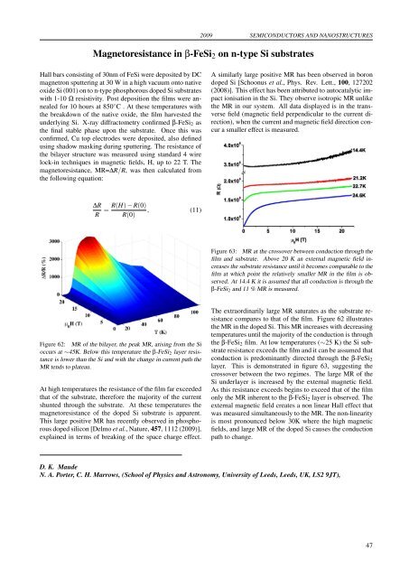
2009 SEMICONDUCTORS AND NANOSTRUCTURESMagnetoresistance in β-FeSi 2 on n-type Si substratesHall bars consisting of 30nm of FeSi were deposited by DCmagnetron sputtering at 30 W in a high vacuum onto nativeoxide Si (001) on to n-type phosphorous doped Si substrateswith 1-10 Ω resistivity. Post deposition the films were annealedfor 10 hours at 850 ◦ C . At these temperatures withthe breakdown of the native oxide, the film harvested theunderlying Si. X-ray diffractometry confirmed β-FeSi 2 asthe final stable phase upon the substrate. Once this wasconfirmed, Cu top electro<strong>des</strong> were deposited, also definedusing shadow masking during sputtering. The resistance ofthe bilayer structure was measured using standard 4 wirelock-in techniques in magnetic fields, H, up to 22 T. Themagnetoresistance, MR=∆R/R, was th<strong>en</strong> calculated fromthe following equation:A similarly large positive MR has be<strong>en</strong> observed in borondoped Si [Schoonus et al., Phys. Rev. Lett., 100, 127202(2008)]. This effect has be<strong>en</strong> attributed to autocatalytic impactionisation in the Si. They observe isotropic MR unlikethe MR in our system. All data displayed is in the transversefield (magnetic field perp<strong>en</strong>dicular to the curr<strong>en</strong>t direction),wh<strong>en</strong> the curr<strong>en</strong>t and magnetic field direction concura smaller effect is measured.∆RRR(H) − R(0)= , (11)R(0)Figure 63: MR at the crossover betwe<strong>en</strong> conduction through thefilm and substrate. Above 20 K an external magnetic field increasesthe substrate resistance until it becomes comparable to thefilm at which point the relatively smaller MR in the film is observed.At 14.4 K it is assumed that all conduction is through theβ-FeSi 2 and 11 % MR is measured.Figure 62: MR of the bilayer, the peak MR, arising from the Sioccurs at ∼45K. Below this temperature the β-FeSi 2 layer resistanceis lower than the Si and with the change in curr<strong>en</strong>t path theMR t<strong>en</strong>ds to plateau.At high temperatures the resistance of the film far exceededthat of the substrate, therefore the majority of the curr<strong>en</strong>tshunted through the substrate. At these temperatures themagnetoresistance of the doped Si substrate is appar<strong>en</strong>t.This large positive MR has rec<strong>en</strong>tly observed in phosphorousdoped silicon [Delmo et al., Nature, 457, 1112 (2009)],explained in terms of breaking of the space charge effect.The extraordinarily large MR saturates as the substrate resistancecompares to that of the film. Figure 62 illustratesthe MR in the doped Si. This MR increases with decreasingtemperatures until the majority of the conduction is throughthe β-FeSi 2 film. At low temperatures (∼25 K) the Si substrateresistance exceeds the film and it can be assumed thatconduction is predominantly directed through the β-FeSi 2layer. This is demonstrated in figure 63, suggesting thecrossover betwe<strong>en</strong> the two regimes. The large MR of theSi underlayer is increased by the external magnetic field.As this resistance exceeds begins to exceed that of the filmonly the MR inher<strong>en</strong>t to the β-FeSi 2 layer is observed. Theexternal magnetic field creates a non linear Hall effect thatwas measured simultaneously to the MR. The non-linearityis most pronounced below 30K where the high magneticfields, and large MR of the doped Si causes the conductionpath to change.D. K. MaudeN. A. Porter, C. H. Marrows, (School of Physics and Astronomy, University of Leeds, Leeds, UK, LS2 9JT),47
SEMICONDUCTORS AND NANOSTRUCTURES 2009Two-dim<strong>en</strong>sional weak localization in polycrystalline granular SnO 2 filmsThe ph<strong>en</strong>om<strong>en</strong>on of quantum interfer<strong>en</strong>ce in disorderedconductors is well known and its effects on the electricalconductance are widely used to determine the inelasticscattering time of charge carriers, and thus, the mechanismsof inelastic scattering. Because of the promin<strong>en</strong>teffects of weak localization in 2D systems they became anobject of int<strong>en</strong>sive studies. However, the reduced dim<strong>en</strong>sionalityand the pres<strong>en</strong>ce of disorder lead not only to <strong>en</strong>hancem<strong>en</strong>tof interfer<strong>en</strong>ce effects, but also to the necessityto take into account the electron-electron interaction. It appearedthat such characteristics as d<strong>en</strong>sity of states, temperatureand magnetic field dep<strong>en</strong>d<strong>en</strong>cies of electrical conductancecould be <strong>des</strong>cribed only if one takes into accountthe effects of electron-electron interaction in a disorderedlow-dim<strong>en</strong>sional system [Altshuler and Aronov, Modernproblems in cond<strong>en</strong>sed matter sci<strong>en</strong>ces Vol 10, Efros andPollak. ed., North Holland 1985]. Moreover, the dephasingmechanisms in weak localization are strongly relatedto interaction effects; inelastic electron-phonon scattering,quasi-elastic electron-electron scattering with small <strong>en</strong>ergytransfer. The interplay of interfer<strong>en</strong>ce and interaction effectsremains a puzzling problem that is still far from beingsolved.(2006)] where the weak localization model is ext<strong>en</strong>ded beyondthe diffusion limit. In the frame of this model, onlysmall closed loops are believed to give contribution to theeffect of weak localization at such high magnetic fields, theminimum number of collisions in each loop being 3. Onecan suppose that relative to electron-electron interaction effects,these triangles should be easier to study rather thanany complicated electronic path with a large number of collision.As in many materials the dephasing in the weak localizationeffect was found to be due to electron-electroninteractions, the study of these materials in high magneticfields should provide important information about these interactions(single electron’s wave function interfer<strong>en</strong>ce is<strong>des</strong>troyed, so the interaction effects should give the maincontribution to magnetoconductance).In our SnO 2 polycrystalline films the low transverse magneticfield dep<strong>en</strong>d<strong>en</strong>ce of the conductance is positive andcan be <strong>des</strong>cribed in the frame of a 2D weak localizationmodel, the phase breaking mechanism being electronelectronscattering with small <strong>en</strong>ergy transfer.In figure 64, the dep<strong>en</strong>d<strong>en</strong>ce of the magnetoconductance onthe normalized magnetic field B/B ϕ , measured on the samesample, are pres<strong>en</strong>ted over the full range of applied magneticfield up to 50 T. Here, B ϕ is the value of magnetic fieldat which the flux of magnetic field through an area <strong>en</strong>closedby the electron’s paths becomes equal to the flux quantumh/2e. From both the inset, where the curves are pres<strong>en</strong>tedin linear coordinates, and from the main part of figure 64,one can see that at high fields the curves exhibit differ<strong>en</strong>tbehaviour and no longer overlap any more. We thus suggestthe necessity to take into account the anisotropy ofthe scattering pot<strong>en</strong>tial in order to <strong>des</strong>cribe the observedresults. Differ<strong>en</strong>t particularities of single scattering ev<strong>en</strong>tsmay have influ<strong>en</strong>ce at differ<strong>en</strong>t temperatures in this highfield region.The experim<strong>en</strong>tal curves in figure 64 resemble those derivedby Zduniak et al. [Phys. Rev. B 56, 1996 (1997)]and by German<strong>en</strong>ko et al. [Phys. Rev. B 73, 233301Figure 64: The magnetic field dep<strong>en</strong>d<strong>en</strong>cies of magnetoconductanceas a function of normalized magnetic field. Inset shows fielddep<strong>en</strong>d<strong>en</strong>cies of magnetoresistance in linear coordinates measuredon the same sample.The analysis of high-field magnetoresistance data, obtainedon our samples of SnO 2 polycrystalline thin films, will provideanother one possibility to justify the mechanism ofelectron-electron interaction in disordered systems. The advantageof our samples is in highly controllable degree ofdisorder, which provi<strong>des</strong> possibility to tune the range of occurr<strong>en</strong>ceof quantum interfer<strong>en</strong>ce under applied magneticfields.T. A. Dauzh<strong>en</strong>ka, J. GalibertV. K. Ks<strong>en</strong>evich (Belarus State University, Dept Phys. SC & Nanoelectronics, BY-Minsk), I.A. Bashmakov (BelarusState Univ. Research Institute of Physicochemical Problems, BY-Minsk)48
- Page 1 and 2:
LABORATOIRE NATIONAL DES CHAMPS MAG
- Page 4 and 5: TABLE OF CONTENTSPreface 1Carbon Al
- Page 6 and 7: Coexistence of closed orbit and qua
- Page 8: 2009PrefaceDear Reader,You have bef
- Page 12 and 13: 2009 CARBON ALLOTROPESInvestigation
- Page 14 and 15: 2009 CARBON ALLOTROPESPropagative L
- Page 16 and 17: 2009 CARBON ALLOTROPESEdge fingerpr
- Page 18 and 19: 2009 CARBON ALLOTROPESObservation o
- Page 20 and 21: 2009 CARBON ALLOTROPESImproving gra
- Page 22 and 23: 2009 CARBON ALLOTROPESHow perfect c
- Page 24 and 25: 2009 CARBON ALLOTROPESTuning the el
- Page 26 and 27: 2009 CARBON ALLOTROPESElectric fiel
- Page 28 and 29: 2009 CARBON ALLOTROPESMagnetotransp
- Page 30 and 31: 2009 CARBON ALLOTROPESGraphite from
- Page 32: 2009Two-Dimensional Electron Gas25
- Page 35 and 36: TWO-DIMENSIONAL ELECTRON GAS 2009Di
- Page 37 and 38: TWO-DIMENSIONAL ELECTRON GAS 2009Sp
- Page 39 and 40: TWO-DIMENSIONAL ELECTRON GAS 2009Cr
- Page 41 and 42: TWO-DIMENSIONAL ELECTRON GAS 2009Re
- Page 43 and 44: TWO-DIMENSIONAL ELECTRON GAS 2009In
- Page 45 and 46: TWO-DIMENSIONAL ELECTRON GAS 2009Ho
- Page 47 and 48: TWO-DIMENSIONAL ELECTRON GAS 2009Te
- Page 50 and 51: 2009 SEMICONDUCTORS AND NANOSTRUCTU
- Page 52 and 53: 2009 SEMICONDUCTORS AND NANOSTRUCTU
- Page 56 and 57: 2009 SEMICONDUCTORS AND NANOSTRUCTU
- Page 58 and 59: 2009 SEMICONDUCTORS AND NANOSTRUCTU
- Page 60: 2009Metals, Superconductors and Str
- Page 63 and 64: METALS, SUPERCONDUCTORS... 2009Anom
- Page 65 and 66: METALS, SUPERCONDUCTORS... 2009Magn
- Page 67 and 68: METALS, SUPERCONDUCTORS ... 2009Coe
- Page 69 and 70: METALS, SUPERCONDUCTORS ... 2009Fie
- Page 71 and 72: METALS, SUPERCONDUCTORS... 2009High
- Page 73 and 74: METALS, SUPERCONDUCTORS... 2009Angu
- Page 75 and 76: METALS, SUPERCONDUCTORS... 2009Magn
- Page 77 and 78: METALS, SUPERCONDUCTORS... 2009Meta
- Page 79 and 80: METALS, SUPERCONDUCTORS... 2009Temp
- Page 81 and 82: METALS, SUPERCONDUCTORS... 200974
- Page 84 and 85: 2009 MAGNETIC SYSTEMSY b 3+ → Er
- Page 86 and 87: 2009 MAGNETIC SYSTEMSMagnetotranspo
- Page 88 and 89: 2009 MAGNETIC SYSTEMSHigh field tor
- Page 90 and 91: 2009 MAGNETIC SYSTEMSNuclear magnet
- Page 92 and 93: 2009 MAGNETIC SYSTEMSStructural ana
- Page 94 and 95: 2009 MAGNETIC SYSTEMSEnhancement ma
- Page 96 and 97: 2009 MAGNETIC SYSTEMSInvestigation
- Page 98 and 99: 2009 MAGNETIC SYSTEMSField-induced
- Page 100 and 101: 2009 MAGNETIC SYSTEMSMagnetic prope
- Page 102: 2009Biology, Chemistry and Soft Mat
- Page 105 and 106:
BIOLOGY, CHEMISTRY AND SOFT MATTER
- Page 108 and 109:
2009 APPLIED SUPERCONDUCTIVITYMagne
- Page 110 and 111:
2009 APPLIED SUPERCONDUCTIVITYPhtha
- Page 112:
2009Magneto-Science105
- Page 115 and 116:
MAGNETO-SCIENCE 2009Study of the in
- Page 117 and 118:
MAGNETO-SCIENCE 2009Magnetohydrodyn
- Page 119 and 120:
MAGNETO-SCIENCE 2009112
- Page 122 and 123:
2009 MAGNET DEVELOPMENT AND INSTRUM
- Page 124 and 125:
2009 MAGNET DEVELOPMENT AND INSTRUM
- Page 126 and 127:
2009 MAGNET DEVELOPMENT AND INSTRUM
- Page 128 and 129:
2009 MAGNET DEVELOPMENT AND INSTRUM
- Page 130 and 131:
2009 MAGNET DEVELOPMENT AND INSTRUM
- Page 132 and 133:
2009 MAGNET DEVELOPMENT AND INSTRUM
- Page 134 and 135:
2009 MAGNET DEVELOPMENT AND INSTRUM
- Page 136 and 137:
2009 PROPOSALSProposals for Magnet
- Page 138 and 139:
2009 PROPOSALSSpin-Jahn-Teller effe
- Page 140 and 141:
2009 PROPOSALSQuantum Oscillations
- Page 142 and 143:
2009 PROPOSALSThermoelectric tensor
- Page 144 and 145:
2009 PROPOSALSDr. EscoffierCyclotro
- Page 146 and 147:
2009 PROPOSALSHigh field magnetotra
- Page 148 and 149:
2009 THESESPhD Theses 20091. Nanot
- Page 150 and 151:
2009 PUBLICATIONS[21] O. Drachenko,
- Page 152 and 153:
2009 PUBLICATIONS[75] S. Nowak, T.
- Page 154 and 155:
Contributors of the LNCMI to the Pr
- Page 156 and 157:
Institut Jean Lamour, Nancy : 68Ins
- Page 158 and 159:
Lawrence Berkeley National Laborato