Mise en page 1 - Laboratoire National des Champs Magnétiques ...
Mise en page 1 - Laboratoire National des Champs Magnétiques ...
Mise en page 1 - Laboratoire National des Champs Magnétiques ...

You also want an ePaper? Increase the reach of your titles
YUMPU automatically turns print PDFs into web optimized ePapers that Google loves.
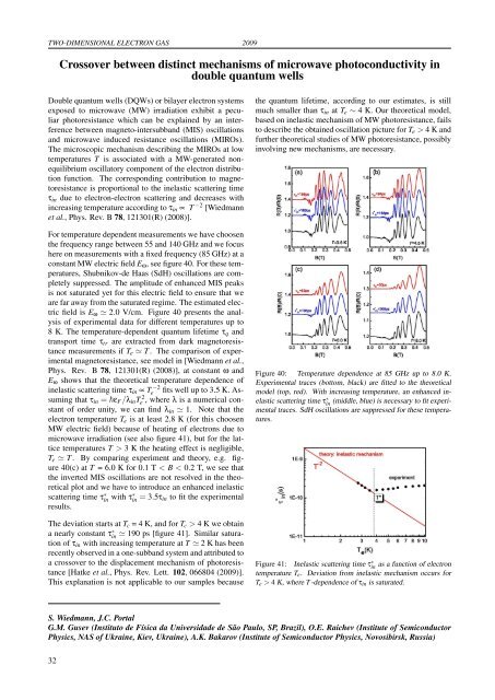
TWO-DIMENSIONAL ELECTRON GAS 2009Crossover betwe<strong>en</strong> distinct mechanisms of microwave photoconductivity indouble quantum wellsDouble quantum wells (DQWs) or bilayer electron systemsexposed to microwave (MW) irradiation exhibit a peculiarphotoresistance which can be explained by an interfer<strong>en</strong>cebetwe<strong>en</strong> magneto-intersubband (MIS) oscillationsand microwave induced resistance oscillations (MIROs).The microscopic mechanism <strong>des</strong>cribing the MIROs at lowtemperatures T is associated with a MW-g<strong>en</strong>erated nonequilibriumoscillatory compon<strong>en</strong>t of the electron distributionfunction. The corresponding contribution to magnetoresistanceis proportional to the inelastic scattering timeτ in due to electron-electron scattering and decreases withincreasing temperature according to τ in ∝ T −2 [Wiedmannet al., Phys. Rev. B 78, 121301(R) (2008)].For temperature dep<strong>en</strong>d<strong>en</strong>t measurem<strong>en</strong>ts we have choos<strong>en</strong>the frequ<strong>en</strong>cy range betwe<strong>en</strong> 55 and 140 GHz and we focushere on measurem<strong>en</strong>ts with a fixed frequ<strong>en</strong>cy (85 GHz) at aconstant MW electric field E ω , see figure 40. For these temperatures,Shubnikov-de Haas (SdH) oscillations are completelysuppressed. The amplitude of <strong>en</strong>hanced MIS peaksis not saturated yet for this electric field to <strong>en</strong>sure that weare far away from the saturated regime. The estimated electricfield is E ω ≃ 2.0 V/cm. Figure 40 pres<strong>en</strong>ts the analysisof experim<strong>en</strong>tal data for differ<strong>en</strong>t temperatures up to8 K. The temperature-dep<strong>en</strong>d<strong>en</strong>t quantum lifetime τ q andtransport time τ tr are extracted from dark magnetoresistancemeasurem<strong>en</strong>ts if T e ≃ T . The comparison of experim<strong>en</strong>talmagnetoresistance, see model in [Wiedmann et al.,Phys. Rev. B 78, 121301(R) (2008)], at constant ω andE ω shows that the theoretical temperature dep<strong>en</strong>d<strong>en</strong>ce ofinelastic scattering time τ in ∝ Te−2 fits well up to 3.5 K. Assumingthat τ in = ε F /λ in Te 2 , where λ is a numerical constantof order unity, we can find λ in ≃ 1. Note that theelectron temperature T e is at least 2.8 K (for this choos<strong>en</strong>MW electric field) because of heating of electrons due tomicrowave irradiation (see also figure 41), but for the latticetemperatures T > 3 K the heating effect is negligible,T e ≃ T . By comparing experim<strong>en</strong>t and theory, e.g. figure40(c) at T = 6.0 K for 0.1 T < B < 0.2 T, we see thatthe inverted MIS oscillations are not resolved in the theoreticalplot and we have to introduce an <strong>en</strong>hanced inelasticscattering time τ ∗ in with τ∗ in = 3.5τ in to fit the experim<strong>en</strong>talresults.The deviation starts at T c = 4 K, and for T c > 4 K we obtaina nearly constant τ ∗ in ≃ 190 ps [figure 41]. Similar saturationof τ in with increasing temperature at T ≃ 2 K has be<strong>en</strong>rec<strong>en</strong>tly observed in a one-subband system and attributed toa crossover to the displacem<strong>en</strong>t mechanism of photoresistance[Hatke et al., Phys. Rev. Lett. 102, 066804 (2009)].This explanation is not applicable to our samples becausethe quantum lifetime, according to our estimates, is stillmuch smaller than τ in at T e ∼ 4 K. Our theoretical model,based on inelastic mechanism of MW photoresistance, failsto <strong>des</strong>cribe the obtained oscillation picture for T e > 4 K andfurther theoretical studies of MW photoresistance, possiblyinvolving new mechanisms, are necessary.Figure 40: Temperature dep<strong>en</strong>d<strong>en</strong>ce at 85 GHz up to 8.0 K.Experim<strong>en</strong>tal traces (bottom, black) are fitted to the theoreticalmodel (top, red). With increasing temperature, an <strong>en</strong>hanced inelasticscattering time τ ∗ in (middle, blue) is necessary to fit experim<strong>en</strong>taltraces. SdH oscillations are suppressed for these temperatures.Figure 41: Inelastic scattering time τ ∗ in as a function of electrontemperature T e . Deviation from inelastic mechanism occurs forT e > 4 K, where T -dep<strong>en</strong>d<strong>en</strong>ce of τ in is saturated.S. Wiedmann, J.C. PortalG.M. Gusev (Instituto de Física da Universidade de São Paulo, SP, Brazil), O.E. Raichev (Institute of SemiconductorPhysics, NAS of Ukraine, Kiev, Ukraine), A.K. Bakarov (Institute of Semiconductor Physics, Novosibirsk, Russia)32