Mise en page 1 - Laboratoire National des Champs Magnétiques ...
Mise en page 1 - Laboratoire National des Champs Magnétiques ...
Mise en page 1 - Laboratoire National des Champs Magnétiques ...

Create successful ePaper yourself
Turn your PDF publications into a flip-book with our unique Google optimized e-Paper software.
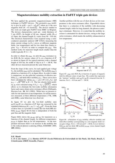
2009 SEMICONDUCTORS AND NANOSTRUCTURESMagnetoresistance mobility extraction in FinFET triple gate devicesWe have applied the geometric magnetoresistance (MR)technique to FinFET devices. The geometric µ MR mobilityis give by ρ(B) = ρ 0 (1 + µ 2 MR B2 ) where ρ 0 is the zeromagnetic field (B = 0) resistivity. The devices studied inthis work are triple-gate FinFET from IMEC in Belgium.The devices characteristics used are: oxide thickness of2 nm (EOT), fin height of 60 nm, channel width (W f in )of 10µm, the channel l<strong>en</strong>gth (L) varies from 90 − 910 nm.The electrical characteristics were acquired using a semiconductorparameter analyzer (HP 4156A) measuring thedrain curr<strong>en</strong>t-voltage I D (V G ) curves at differ<strong>en</strong>t magneticfields, low temperatures and for low drain bias (linear region:V DS = 50 mV) in order to compute the µ MR . Thismethod works for transistor l<strong>en</strong>gth much smaller than thewidth (typically W/L > 5).Another problem with the use of short devices at low temperaturesis the series resistance effect. Figure66(b) showsthat there is a reduction of the mobility with decreasingchannel l<strong>en</strong>gth, while for long channels, the phonon scatteringis dominant. However, it is noted that the mobility increasesis att<strong>en</strong>uated for shorter devices, owing to the largeseries resistance, which masks the mobility <strong>en</strong>hancem<strong>en</strong>t atlow temperature.In order to obtain the µ MR , we plot the µ MR resistance ratioR(B)/R 0 for various values of V G as a function of B 2as shown in figure 65 for typical transistor with a channell<strong>en</strong>gth of 410 nm, fin width of 10µ m at T = 100 K. Theother devices measured pres<strong>en</strong>t the same behaviour.From the slope of this curve, for each applied gate voltageV G , the mobility µ MR can be calculated. The mobility µ MR isplotted as a function of V G in figure 66(a). In order to makea comparison, we also plott the variations of effective mobilityµ e f f and field-effect mobility µ FE . These curves havebe<strong>en</strong> calculated by taking µ FE = gm/((W/L)C ox V D ) andµ e f f = √ µ 0 − µ FE at B = 0. The low electric-field mobilityµ 0 were extracted using Y (V G ) = I D / √ gm(V G ), whichallows us to eliminate the first-order mobility att<strong>en</strong>uationfactor and source-drain series resistance effects [Ghibaudo,Electron Lett. 24, 543 (1988)]. While here we pres<strong>en</strong>t resultsfor one transistor at one temperature, for all the transistorsmeasured, at three differ<strong>en</strong>t temperatures (77K, 100Kand 200K), same behaviour was observed.Figure 65: µ MR ratio R(B)/R 0 in function of square of magneticfield for differ<strong>en</strong>t values of gate bias. The symbol line repres<strong>en</strong>tsthe “intrinsic” mobility ratio µ 0 (0)/µ 0 (B) extracted from the Y–function. For L = 410 nm and T = 100 K.In figure 65 we plot the low-field mobility ratioµ 0 (0)/µ 0 (B) as a function of B 2 that was extracted by thestandard relation µ 0 (B) = µ 0 /(1+µ 2 0,MR B2 ). From the slopeof these lines it is possible to extract the low-field MR mobilityµ 0,MR (figure 66 (b) that is indep<strong>en</strong>d<strong>en</strong>t of both thegate bias and the magnetic field.Figure 66(b) shows the µ 0,MR and µ 0 for transistors as afunction of the channel l<strong>en</strong>gth, for differ<strong>en</strong>t temperatures.µ 0,MR is higher than µ 0 for all temperatures. As the temperaturedecreases there is an increase in the mobility dueto the reduced phonon scattering [Ohata, ESSDERC 2004,109 (2004)].Figure 66: a)Variations of µ MR mobility, effective mobility andfield effect mobility (corresponding to a zero magnetic field) versusgate voltage. For L = 410 nm and T = 100 K. b) Low-field mobilityµ 0 and low-field, MR mobility µ 0,MR versus channel l<strong>en</strong>gthat differ<strong>en</strong>t temperaturesD.K. MaudeC. D. G. dos Santos , J. A. Martino (EPUSP- Escola Politécnica da Universidade de São Paulo, São Paulo, Brazil), S.Cristoloveanu (IMEP, Gr<strong>en</strong>oble, France)49