2009 SEMICONDUCTORS AND NANOSTRUCTURESMagnetoresistance mobility extraction in FinFET triple gate devicesWe have applied the geometric magnetoresistance (MR)technique to FinFET devices. The geometric µ MR mobilityis give by ρ(B) = ρ 0 (1 + µ 2 MR B2 ) where ρ 0 is the zeromagnetic field (B = 0) resistivity. The devices studied inthis work are triple-gate FinFET from IMEC in Belgium.The devices characteristics used are: oxide thickness of2 nm (EOT), fin height of 60 nm, channel width (W f in )of 10µm, the channel l<strong>en</strong>gth (L) varies from 90 − 910 nm.The electrical characteristics were acquired using a semiconductorparameter analyzer (HP 4156A) measuring thedrain curr<strong>en</strong>t-voltage I D (V G ) curves at differ<strong>en</strong>t magneticfields, low temperatures and for low drain bias (linear region:V DS = 50 mV) in order to compute the µ MR . Thismethod works for transistor l<strong>en</strong>gth much smaller than thewidth (typically W/L > 5).Another problem with the use of short devices at low temperaturesis the series resistance effect. Figure66(b) showsthat there is a reduction of the mobility with decreasingchannel l<strong>en</strong>gth, while for long channels, the phonon scatteringis dominant. However, it is noted that the mobility increasesis att<strong>en</strong>uated for shorter devices, owing to the largeseries resistance, which masks the mobility <strong>en</strong>hancem<strong>en</strong>t atlow temperature.In order to obtain the µ MR , we plot the µ MR resistance ratioR(B)/R 0 for various values of V G as a function of B 2as shown in figure 65 for typical transistor with a channell<strong>en</strong>gth of 410 nm, fin width of 10µ m at T = 100 K. Theother devices measured pres<strong>en</strong>t the same behaviour.From the slope of this curve, for each applied gate voltageV G , the mobility µ MR can be calculated. The mobility µ MR isplotted as a function of V G in figure 66(a). In order to makea comparison, we also plott the variations of effective mobilityµ e f f and field-effect mobility µ FE . These curves havebe<strong>en</strong> calculated by taking µ FE = gm/((W/L)C ox V D ) andµ e f f = √ µ 0 − µ FE at B = 0. The low electric-field mobilityµ 0 were extracted using Y (V G ) = I D / √ gm(V G ), whichallows us to eliminate the first-order mobility att<strong>en</strong>uationfactor and source-drain series resistance effects [Ghibaudo,Electron Lett. 24, 543 (1988)]. While here we pres<strong>en</strong>t resultsfor one transistor at one temperature, for all the transistorsmeasured, at three differ<strong>en</strong>t temperatures (77K, 100Kand 200K), same behaviour was observed.Figure 65: µ MR ratio R(B)/R 0 in function of square of magneticfield for differ<strong>en</strong>t values of gate bias. The symbol line repres<strong>en</strong>tsthe “intrinsic” mobility ratio µ 0 (0)/µ 0 (B) extracted from the Y–function. For L = 410 nm and T = 100 K.In figure 65 we plot the low-field mobility ratioµ 0 (0)/µ 0 (B) as a function of B 2 that was extracted by thestandard relation µ 0 (B) = µ 0 /(1+µ 2 0,MR B2 ). From the slopeof these lines it is possible to extract the low-field MR mobilityµ 0,MR (figure 66 (b) that is indep<strong>en</strong>d<strong>en</strong>t of both thegate bias and the magnetic field.Figure 66(b) shows the µ 0,MR and µ 0 for transistors as afunction of the channel l<strong>en</strong>gth, for differ<strong>en</strong>t temperatures.µ 0,MR is higher than µ 0 for all temperatures. As the temperaturedecreases there is an increase in the mobility dueto the reduced phonon scattering [Ohata, ESSDERC 2004,109 (2004)].Figure 66: a)Variations of µ MR mobility, effective mobility andfield effect mobility (corresponding to a zero magnetic field) versusgate voltage. For L = 410 nm and T = 100 K. b) Low-field mobilityµ 0 and low-field, MR mobility µ 0,MR versus channel l<strong>en</strong>gthat differ<strong>en</strong>t temperaturesD.K. MaudeC. D. G. dos Santos , J. A. Martino (EPUSP- Escola Politécnica da Universidade de São Paulo, São Paulo, Brazil), S.Cristoloveanu (IMEP, Gr<strong>en</strong>oble, France)49
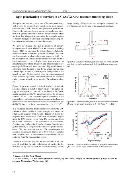
SEMICONDUCTORS AND NANOSTRUCTURES 2009Spin polarization of carriers in a GaAs/GaAlAs resonant tunneling diodeSpin polarized carrier systems are of interest particularlywith a view to polarized spin injection for giant magnetotoresistance(GMR) devices and spintronics applications.However, for various physical reasons, spin polarized injectionis in g<strong>en</strong>eral difficult to achieve in real devices. Herewe show that it is possible to monitor the spin polarizationof carriers throughout a resonant tunneling dio<strong>des</strong> using polarizationresolved micro-photoluminesc<strong>en</strong>ce.We have investigated the spin polarization of carriersin asymmetrical n-i-n GaAs/GaAlAs resonant tunnelingdio<strong>des</strong> (RTD) by analyzing the polarized resolved photoluminesc<strong>en</strong>cefrom both GaAs quantum well (QW) and contactlayers under applied voltage and magnetic field. Forthe measurem<strong>en</strong>ts a micro-photoluminesc<strong>en</strong>ce setup with alow temperature x − y − z displacem<strong>en</strong>t stage was used tosimultaneously perform transport and photoluminesc<strong>en</strong>ceon single RTD etched mesa structure. Figure 67 shows aschematic band diagram of our device under forward biasvoltage, light excitation, and magnetic field parallel to thetunnel curr<strong>en</strong>t. Under applied bias, the photo-g<strong>en</strong>eratedholes from the top contact can tunnel through the structureand recombine with electrons into the QW and contact layers.Figure 68 pres<strong>en</strong>ts typical polarized resolved photoluminesc<strong>en</strong>cespectra at 0.195 V bias voltage. The higher <strong>en</strong>ergyemission peak (∼ 1.605 eV) is attributed to the fundam<strong>en</strong>talquantum well (QW) transition whereas the emissionaround 1.52 eV is due to various optical transitions in thecontact layers including the indirect recombination betwe<strong>en</strong>free holes and electrons in the two dim<strong>en</strong>sional electron gas(h-2DEG) formed at the accumulation layer (∼ 1.512 eV).charge d<strong>en</strong>sity, filling factors and spin polarization of thetwo-dim<strong>en</strong>sional gas formed in the accumulation layer.Figure 67: Schematic band diagram of our device under forwardbias, light excitation and magnetic field parallel to the tunnel curr<strong>en</strong>t.Figure 68: A repres<strong>en</strong>tative photoluminesc<strong>en</strong>ce spectra from theQW and contact layers measured at B = 19 T and T = 4.2 K.In a magnetic field the photoluminesc<strong>en</strong>ce from the QWand contact layers shifts to higher <strong>en</strong>ergies and shows oscillationsin int<strong>en</strong>sity (not shown). Figure 69 shows themagnetic field dep<strong>en</strong>d<strong>en</strong>ce of circular polarization degreefrom the QW, contact layers (total PL spectra) and fromthe h-2DEG emission. The polarization of the carriers,P = (I σ+ −I σ− )/(I σ+ +I σ− ), can be obtained from the integratedint<strong>en</strong>sity of the polarization resolved photoluminesc<strong>en</strong>ce.We have observed that the QW emission pres<strong>en</strong>tsnegative polarization degree up to 55% which oscillateswith magnetic field. A similar behavior is observed for theemission from the GaAs contact layers.To further understand this data we are curr<strong>en</strong>tly in the processof modeling the spin polarization of carriers in thestructure taking into account the carrier tunneling, carrierFigure 69: Magnetic field dep<strong>en</strong>d<strong>en</strong>ce of spin polarization of theQW, GaAs contact layers and from the h-2DEG emissions.J. Kunc, M. Orlita, D. K. MaudeY. Galvão Gobato, L.F. dos Santos (Federal University of São Carlos, Brazil), M. H<strong>en</strong>ini (School of Physics and Astronomy,University of Nottingham, UK)50
- Page 1 and 2:
LABORATOIRE NATIONAL DES CHAMPS MAG
- Page 4 and 5:
TABLE OF CONTENTSPreface 1Carbon Al
- Page 6 and 7: Coexistence of closed orbit and qua
- Page 8: 2009PrefaceDear Reader,You have bef
- Page 12 and 13: 2009 CARBON ALLOTROPESInvestigation
- Page 14 and 15: 2009 CARBON ALLOTROPESPropagative L
- Page 16 and 17: 2009 CARBON ALLOTROPESEdge fingerpr
- Page 18 and 19: 2009 CARBON ALLOTROPESObservation o
- Page 20 and 21: 2009 CARBON ALLOTROPESImproving gra
- Page 22 and 23: 2009 CARBON ALLOTROPESHow perfect c
- Page 24 and 25: 2009 CARBON ALLOTROPESTuning the el
- Page 26 and 27: 2009 CARBON ALLOTROPESElectric fiel
- Page 28 and 29: 2009 CARBON ALLOTROPESMagnetotransp
- Page 30 and 31: 2009 CARBON ALLOTROPESGraphite from
- Page 32: 2009Two-Dimensional Electron Gas25
- Page 35 and 36: TWO-DIMENSIONAL ELECTRON GAS 2009Di
- Page 37 and 38: TWO-DIMENSIONAL ELECTRON GAS 2009Sp
- Page 39 and 40: TWO-DIMENSIONAL ELECTRON GAS 2009Cr
- Page 41 and 42: TWO-DIMENSIONAL ELECTRON GAS 2009Re
- Page 43 and 44: TWO-DIMENSIONAL ELECTRON GAS 2009In
- Page 45 and 46: TWO-DIMENSIONAL ELECTRON GAS 2009Ho
- Page 47 and 48: TWO-DIMENSIONAL ELECTRON GAS 2009Te
- Page 50 and 51: 2009 SEMICONDUCTORS AND NANOSTRUCTU
- Page 52 and 53: 2009 SEMICONDUCTORS AND NANOSTRUCTU
- Page 54 and 55: 2009 SEMICONDUCTORS AND NANOSTRUCTU
- Page 58 and 59: 2009 SEMICONDUCTORS AND NANOSTRUCTU
- Page 60: 2009Metals, Superconductors and Str
- Page 63 and 64: METALS, SUPERCONDUCTORS... 2009Anom
- Page 65 and 66: METALS, SUPERCONDUCTORS... 2009Magn
- Page 67 and 68: METALS, SUPERCONDUCTORS ... 2009Coe
- Page 69 and 70: METALS, SUPERCONDUCTORS ... 2009Fie
- Page 71 and 72: METALS, SUPERCONDUCTORS... 2009High
- Page 73 and 74: METALS, SUPERCONDUCTORS... 2009Angu
- Page 75 and 76: METALS, SUPERCONDUCTORS... 2009Magn
- Page 77 and 78: METALS, SUPERCONDUCTORS... 2009Meta
- Page 79 and 80: METALS, SUPERCONDUCTORS... 2009Temp
- Page 81 and 82: METALS, SUPERCONDUCTORS... 200974
- Page 84 and 85: 2009 MAGNETIC SYSTEMSY b 3+ → Er
- Page 86 and 87: 2009 MAGNETIC SYSTEMSMagnetotranspo
- Page 88 and 89: 2009 MAGNETIC SYSTEMSHigh field tor
- Page 90 and 91: 2009 MAGNETIC SYSTEMSNuclear magnet
- Page 92 and 93: 2009 MAGNETIC SYSTEMSStructural ana
- Page 94 and 95: 2009 MAGNETIC SYSTEMSEnhancement ma
- Page 96 and 97: 2009 MAGNETIC SYSTEMSInvestigation
- Page 98 and 99: 2009 MAGNETIC SYSTEMSField-induced
- Page 100 and 101: 2009 MAGNETIC SYSTEMSMagnetic prope
- Page 102: 2009Biology, Chemistry and Soft Mat
- Page 105 and 106: BIOLOGY, CHEMISTRY AND SOFT MATTER
- Page 108 and 109:
2009 APPLIED SUPERCONDUCTIVITYMagne
- Page 110 and 111:
2009 APPLIED SUPERCONDUCTIVITYPhtha
- Page 112:
2009Magneto-Science105
- Page 115 and 116:
MAGNETO-SCIENCE 2009Study of the in
- Page 117 and 118:
MAGNETO-SCIENCE 2009Magnetohydrodyn
- Page 119 and 120:
MAGNETO-SCIENCE 2009112
- Page 122 and 123:
2009 MAGNET DEVELOPMENT AND INSTRUM
- Page 124 and 125:
2009 MAGNET DEVELOPMENT AND INSTRUM
- Page 126 and 127:
2009 MAGNET DEVELOPMENT AND INSTRUM
- Page 128 and 129:
2009 MAGNET DEVELOPMENT AND INSTRUM
- Page 130 and 131:
2009 MAGNET DEVELOPMENT AND INSTRUM
- Page 132 and 133:
2009 MAGNET DEVELOPMENT AND INSTRUM
- Page 134 and 135:
2009 MAGNET DEVELOPMENT AND INSTRUM
- Page 136 and 137:
2009 PROPOSALSProposals for Magnet
- Page 138 and 139:
2009 PROPOSALSSpin-Jahn-Teller effe
- Page 140 and 141:
2009 PROPOSALSQuantum Oscillations
- Page 142 and 143:
2009 PROPOSALSThermoelectric tensor
- Page 144 and 145:
2009 PROPOSALSDr. EscoffierCyclotro
- Page 146 and 147:
2009 PROPOSALSHigh field magnetotra
- Page 148 and 149:
2009 THESESPhD Theses 20091. Nanot
- Page 150 and 151:
2009 PUBLICATIONS[21] O. Drachenko,
- Page 152 and 153:
2009 PUBLICATIONS[75] S. Nowak, T.
- Page 154 and 155:
Contributors of the LNCMI to the Pr
- Page 156 and 157:
Institut Jean Lamour, Nancy : 68Ins
- Page 158 and 159:
Lawrence Berkeley National Laborato