Mise en page 1 - Laboratoire National des Champs Magnétiques ...
Mise en page 1 - Laboratoire National des Champs Magnétiques ...
Mise en page 1 - Laboratoire National des Champs Magnétiques ...

You also want an ePaper? Increase the reach of your titles
YUMPU automatically turns print PDFs into web optimized ePapers that Google loves.
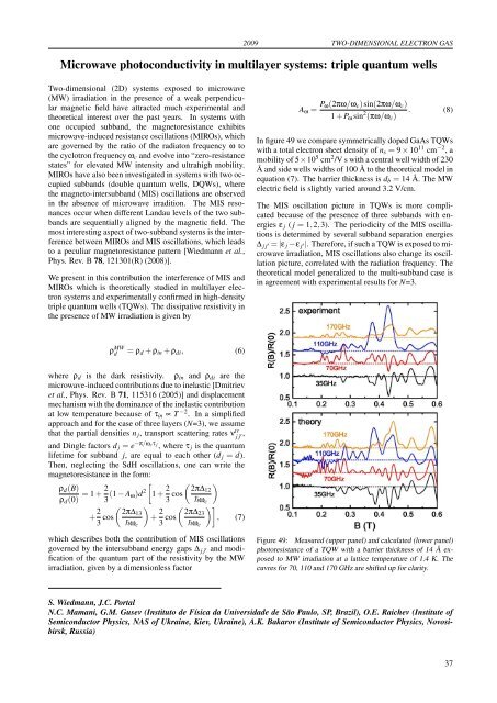
2009 TWO-DIMENSIONAL ELECTRON GASMicrowave photoconductivity in multilayer systems: triple quantum wellsTwo-dim<strong>en</strong>sional (2D) systems exposed to microwave(MW) irradiation in the pres<strong>en</strong>ce of a weak perp<strong>en</strong>dicularmagnetic field have attracted much experim<strong>en</strong>tal andtheoretical interest over the past years. In systems withone occupied subband, the magnetoresistance exhibitsmicrowave-induced resistance oscillations (MIROs), whichare governed by the ratio of the radiaton frequ<strong>en</strong>cy ω tothe cyclotron frequ<strong>en</strong>cy ω c and evolve into “zero-resistancestates” for elevated MW int<strong>en</strong>sity and ultrahigh mobility.MIROs have also be<strong>en</strong> investigated in systems with two occupiedsubbands (double quantum wells, DQWs), wherethe magneto-intersubband (MIS) oscillations are observedin the abs<strong>en</strong>ce of microwave irradition. The MIS resonancesoccur wh<strong>en</strong> differ<strong>en</strong>t Landau levels of the two subbandsare sequ<strong>en</strong>tially aligned by the magnetic field. Themost interesting aspect of two-subband systems is the interfer<strong>en</strong>cebetwe<strong>en</strong> MIROs and MIS oscillations, which leadsto a peculiar magnetoresistance pattern [Wiedmann et al.,Phys. Rev. B 78, 121301(R) (2008)].We pres<strong>en</strong>t in this contribution the interfer<strong>en</strong>ce of MIS andMIROs which is theoretically studied in multilayer electronsystems and experim<strong>en</strong>tally confirmed in high-d<strong>en</strong>sitytriple quantum wells (TQWs). The dissipative resistivity inthe pres<strong>en</strong>ce of MW irradiation is giv<strong>en</strong> byA ω = P ω(2πω/ω c )sin(2πω/ω c )1 + P ω sin 2 . (8)(πω/ω c )In figure 49 we compare symmetrically doped GaAs TQWswith a total electron sheet d<strong>en</strong>sity of n s = 9 × 10 11 cm −2 , amobility of 5×10 5 cm 2 /V s with a c<strong>en</strong>tral well width of 230Å and side wells widths of 100 Å to the theoretical model inequation (7). The barrier thickness is d b = 14 Å. The MWelectric field is slightly varied around 3.2 V/cm.The MIS oscillation picture in TQWs is more complicatedbecause of the pres<strong>en</strong>ce of three subbands with <strong>en</strong>ergiesε j ( j = 1,2,3). The periodicity of the MIS oscillationsis determined by several subband separation <strong>en</strong>ergies∆ j j ′ = |ε j −ε j ′|. Therefore, if such a TQW is exposed to microwaveirradiation, MIS oscillations also change its oscillationpicture, correlated with the radiation frequ<strong>en</strong>cy. Thetheoretical model g<strong>en</strong>eralized to the multi-subband case isin agreem<strong>en</strong>t with experim<strong>en</strong>tal results for N=3.ρ MWd = ρ d + ρ in + ρ di , (6)where ρ d is the dark resistivity. ρ in and ρ di are themicrowave-induced contributions due to inelastic [Dmitrievet al., Phys. Rev. B 71, 115316 (2005)] and displacem<strong>en</strong>tmechanism with the dominance of the inelastic contributionat low temperature because of τ in ∝ T −2 . In a simplifiedapproach and for the case of three layers (N=3), we assumethat the partial d<strong>en</strong>sities n j , transport scattering rates ν trj j ′ ,and Dingle factors d j = e −π/ω cτ j , where τ j is the quantumlifetime for subband j, are equal to each other (d j = d).Th<strong>en</strong>, neglecting the SdH oscillations, one can write themagnetoresistance in the form:ρ d (B)ρ d (0) = 1 + 2 [3 (1 − A ω)d 2 1 + 2 ( )3 cos 2π∆12ω c+ 2 ( )3 cos 2π∆13+ 2 ( )]ω c 3 cos 2π∆23, (7)ω cwhich <strong>des</strong>cribes both the contribution of MIS oscillationsgoverned by the intersubband <strong>en</strong>ergy gaps ∆ j j ′ and modificationof the quantum part of the resistivity by the MWirradiation, giv<strong>en</strong> by a dim<strong>en</strong>sionless factorFigure 49: Measured (upper panel) and calculated (lower panel)photoresistance of a TQW with a barrier thickness of 14 Å exposedto MW irradiation at a lattice temperature of 1.4 K. Thecuvres for 70, 110 and 170 GHz are shifted up for clarity.S. Wiedmann, J.C. PortalN.C. Mamani, G.M. Gusev (Instituto de Física da Universidade de São Paulo, SP, Brazil), O.E. Raichev (Institute ofSemiconductor Physics, NAS of Ukraine, Kiev, Ukraine), A.K. Bakarov (Institute of Semiconductor Physics, Novosibirsk,Russia)37