- Page 2 and 3:
Starting Electronics i
- Page 4 and 5:
Starting Electronics Keith Brindley
- Page 6 and 7:
Contents Contents Preface vi 1. The
- Page 8 and 9:
The very first steps 1 The very fir
- Page 10 and 11:
The very first steps potential rewa
- Page 12 and 13:
The very first steps Photo 1.2 tool
- Page 14 and 15:
The very first steps that electrici
- Page 16 and 17:
The very first steps Going back to
- Page 18 and 19:
The very first steps tially exist.
- Page 20 and 21:
The very first steps by a scientist
- Page 22 and 23:
The very first steps Hint: Ohm’s
- Page 24 and 25:
The very first steps Electronic com
- Page 26 and 27:
The very first steps Larger values
- Page 28 and 29:
The very first steps Time out That
- Page 30 and 31:
On the boards 2 On the boards In th
- Page 32 and 33:
On the boards If you are following
- Page 34 and 35:
On the boards Hint: The theoretical
- Page 36 and 37:
On the boards Photo 2.2 Inside brea
- Page 38 and 39:
On the boards Down the edges of the
- Page 40 and 41:
On the boards Hint: The multi-meter
- Page 42 and 43:
On the boards of leads should be su
- Page 44 and 45:
On the boards it gets older and sta
- Page 46 and 47:
On the boards Hint: The bands group
- Page 48 and 49:
On the boards In practice, you migh
- Page 50 and 51:
On the boards called just ohmmeter)
- Page 52 and 53:
On the boards ends. We say resistor
- Page 54 and 55:
On the boards we would get: and thi
- Page 56 and 57:
On the boards Figure 2.9 A comparat
- Page 58 and 59:
Measuring current and voltage 3 Mea
- Page 60 and 61:
Measuring current and voltage forme
- Page 62 and 63:
Measuring current and voltage Netwo
- Page 64 and 65:
Measuring current and voltage Netwo
- Page 66 and 67:
Measuring current and voltage Did y
- Page 68 and 69:
Measuring current and voltage Figur
- Page 70 and 71:
Measuring current and voltage Figur
- Page 72 and 73:
Practically there Measuring current
- Page 74 and 75:
Measuring current and voltage Take
- Page 76 and 77:
Measuring current and voltage Figur
- Page 78 and 79:
Measuring current and voltage Take
- Page 80 and 81:
Measuring current and voltage Figur
- Page 82 and 83:
Measuring current and voltage Hint:
- Page 84 and 85:
Capacitors 4 Capacitors You need a
- Page 86 and 87:
Capacitors Capacitors We’re going
- Page 88 and 89:
Capacitors In our experiments in th
- Page 90 and 91:
Capacitors Figure 4.4 A simple resi
- Page 92 and 93:
Capacitors Time (seconds) 5 10 15 2
- Page 94 and 95:
Capacitors Time (seconds) 5 10 15 2
- Page 96 and 97:
Capacitors In a capacitor circuit l
- Page 98 and 99:
Capacitors Figure 4.11 An experimen
- Page 100 and 101:
Capacitors Time (seconds) Voltage (
- Page 102 and 103:
Capacitors plates of the capacitor
- Page 104 and 105:
Capacitors where ε is the permitti
- Page 106 and 107:
ICs oscillators and filters 5 ICs,
- Page 108 and 109:
ICs oscillators and filters Photo 5
- Page 110 and 111:
ICs oscillators and filters We’ve
- Page 112 and 113:
ICs oscillators and filters an osci
- Page 114 and 115:
ICs oscillators and filters (a) (b)
- Page 116 and 117:
ICs oscillators and filters Ouch, t
- Page 118 and 119:
ICs oscillators and filters output
- Page 120 and 121:
ICs oscillators and filters Value o
- Page 122 and 123:
ICs oscillators and filters voltage
- Page 124 and 125:
ICs oscillators and filters Value o
- Page 126 and 127: ICs oscillators and filters Figure
- Page 128 and 129: ICs oscillators and filters simple
- Page 130 and 131: Diodes I 6 Diodes I We’re going t
- Page 132 and 133: Diodes I Photo 6.1 A horizontal pre
- Page 134 and 135: Diodes I Now, with a resistance of
- Page 136 and 137: Diodes I here. We needn’t know an
- Page 138 and 139: Diodes I Figure 6.9 The breadboard
- Page 140 and 141: Diodes I but we never said it was a
- Page 142 and 143: Diodes I Current (mA) Voltage (V) 0
- Page 144 and 145: Diodes I voltages, reverse currents
- Page 146 and 147: Diodes I battery voltage of 9 V sim
- Page 148 and 149: Diodes I Figure 6.17 The circuit, w
- Page 150 and 151: Diodes I Figure 6.19 My results fro
- Page 152 and 153: Diodes II 7 Diodes II In the last c
- Page 154 and 155: Diodes II the same experiment we di
- Page 156 and 157: Diodes II We need to draw diode cha
- Page 158 and 159: Diodes II Generally, diodes don’t
- Page 160 and 161: Diodes II Diode voltage (VD) Resist
- Page 162 and 163: Diodes II Diode circuits We’re no
- Page 164 and 165: Diodes II Figure 7.9 Waveforms show
- Page 166 and 167: Diodes II Filter tips Although we
- Page 168 and 169: Diodes II We’ve already seen a de
- Page 170 and 171: Diodes II as that from a 230 V a.c.
- Page 172 and 173: Diodes II Figure 7.19 The same circ
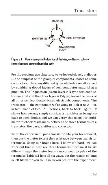
- Page 174 and 175: Transistors 8 Transistors In previo
- Page 178 and 179: Transistors Black meter lead Red me
- Page 180 and 181: Transistors Well, as mentioned earl
- Page 182 and 183: Transistors Figure 8.8 A breadboard
- Page 184 and 185: Transistors In effect, the transist
- Page 186 and 187: Transistors Figure 8.10 transistors
- Page 188 and 189: Transistors Hint: Yes, that’s rig
- Page 190 and 191: Transistors These two operational m
- Page 192 and 193: Analogue integrated circuits 9 Anal
- Page 194 and 195: Analogue integrated circuits circui
- Page 196 and 197: Analogue integrated circuits Figure
- Page 198 and 199: Building on blocs Analogue integrat
- Page 200 and 201: Analogue integrated circuits Figure
- Page 202 and 203: Analogue integrated circuits As the
- Page 204 and 205: Analogue integrated circuits Figure
- Page 206 and 207: Analogue integrated circuits circui
- Page 208 and 209: Analogue integrated circuits Figure
- Page 210 and 211: Analogue integrated circuits Figure
- Page 212 and 213: Analogue integrated circuits an app
- Page 214 and 215: Digital integrated circuits I 10 Di
- Page 216 and 217: Digital integrated circuits I Logic
- Page 218 and 219: Digital integrated circuits I If we
- Page 220 and 221: Digital integrated circuits I Figur
- Page 222 and 223: Digital integrated circuits I It’
- Page 224 and 225: Digital integrated circuits I Figur
- Page 226 and 227:
Digital integrated circuits I Figur
- Page 228 and 229:
Digital integrated circuits I The t
- Page 230 and 231:
Digital integrated circuits I Trans
- Page 232 and 233:
Digital integrated circuits I Figur
- Page 234 and 235:
Digital integrated circuits I Figur
- Page 236 and 237:
Digital integrated circuits I Figur
- Page 238 and 239:
Digital integrated circuits I going
- Page 240 and 241:
Digital integrated circuits I OR an
- Page 242 and 243:
Digital integrated circuits I For t
- Page 244 and 245:
Digital integrated circuits I Figur
- Page 246 and 247:
Digital integrated circuits I Figur
- Page 248 and 249:
Digital integrated circuits II 11 D
- Page 250 and 251:
Digital integrated circuits II A se
- Page 252 and 253:
Shutting the ’stable gate Digital
- Page 254 and 255:
Digital integrated circuits II gate
- Page 256 and 257:
Digital integrated circuits II In o
- Page 258 and 259:
Digital integrated circuits II Figu
- Page 260 and 261:
Digital integrated circuits II Swit
- Page 262 and 263:
Digital integrated circuits II The
- Page 264 and 265:
Digital integrated circuits II Figu
- Page 266 and 267:
Digital integrated circuits II Figu
- Page 268 and 269:
Open the black box Digital integrat
- Page 270 and 271:
Digital integrated circuits II Figu
- Page 272 and 273:
Digital integrated circuits II Ther
- Page 274 and 275:
Glossary Glossary 180 ° out-of-pha
- Page 276 and 277:
Glossary bode plots method of showi
- Page 278 and 279:
Glossary decibels logarithmic units
- Page 280 and 281:
Glossary integrated circuit a semic
- Page 282 and 283:
Glossary peak voltage the voltage m
- Page 284 and 285:
Glossary squarewave a signal which
- Page 286 and 287:
Glossary Components used Resistors
- Page 288 and 289:
Glossary Index A ampere, 9 AND gate


![[Gray___Meyer]_Analysis_and_Design_of_Analog_Integrated_Circuits_5th_cropped](https://img.yumpu.com/55897897/1/190x255/gray-meyer-analysis-and-design-of-analog-integrated-circuits-5th-cropped.jpg?quality=85)