

Electronic Material Properties - und Geowissenschaften ...
Electronic Material Properties - und Geowissenschaften ...
Electronic Material Properties - und Geowissenschaften ...

Create successful ePaper yourself
Turn your PDF publications into a flip-book with our unique Google optimized e-Paper software.
∆ = 0<br />
−<br />
exhibiting dominance of space charge effects at low barriers. At low voltages<br />
up to 0.1 V all I-V-characteristics show an Ohmic-like j ≈ V dependence. This Ohmic<br />
regime is followed by an exponential increase of the current density with the voltage<br />
up to the built-in voltage VBI = 0.81 eV corresponding to the difference in the workfunctions<br />
of the electrodes. This increase can be attributed to a diffusive charge<br />
carrier transport against the weakened electric field in the organic material. If a high<br />
injection barrier is present, the following current-density increase is also exponential<br />
due to the barrier modification by the electric field at the interface. After all, when the<br />
injection barrier at the injecting electrode falls below ∆ crit the calcium contact can<br />
supply more charge carriers than the bulk of the organic semiconductor can<br />
transport. That is why all the I-V-characteristics end up in the space charge limited<br />
regime.<br />
In the case of high injection barriers the approximate analytic consideration results in<br />
the I-V-characteristic of the system which reads<br />
⎛ eV ⎞<br />
− exp⎜−<br />
⎟ −1<br />
V + V ⎛ ∆ ⎞<br />
BI<br />
eff<br />
exp⎜<br />
⎟ ⎝ kT<br />
j = −eµ<br />
⎠<br />
s N<br />
⎜<br />
−<br />
⎟<br />
, (2)<br />
L ⎝ kT ⎠ ⎛ e(<br />
V + VBI<br />
) ⎞<br />
exp⎜−<br />
⎟ −1<br />
⎝ kT ⎠<br />
where µ s is the mobility of electrons in the insulator and the modified barrier equals<br />
−<br />
−<br />
∆eff<br />
= ∆ + eε lTFFs<br />
( −L<br />
/ 2)<br />
. The agreement of this formula with numerical calculations is<br />
perfect for reverse and forward bias until the space charge effects become dominant.<br />
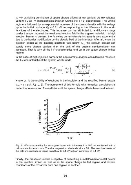
Fig. 1: I-V-characteristics for an organic layer with thickness L = 100 nm contacted with a<br />
calcium electrode at x = -L/2 and a magnesium electrode at x = L/2. The injection barrier of<br />
the calcium electrode is varied from 0 eV to 0.4 eV with an increment of 0.1 eV.<br />
Finally, the presented model is capable of describing a metal/insulator/metal device<br />
in the injection limited as well as in the space charge limited regime and reveals<br />
conditions of the crossover from one regime to another.<br />
- 98 -