

Electronic Material Properties - und Geowissenschaften ...
Electronic Material Properties - und Geowissenschaften ...
Electronic Material Properties - und Geowissenschaften ...

Create successful ePaper yourself
Turn your PDF publications into a flip-book with our unique Google optimized e-Paper software.
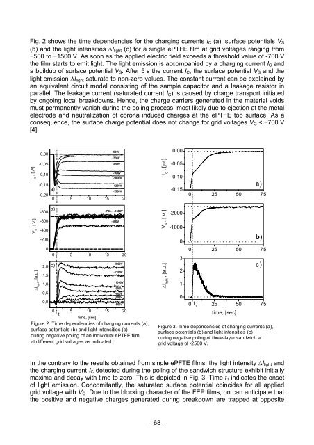
Fig. 2 shows the time dependencies for the charging currents IC (a), surface potentials VS<br />
(b) and the light intensities ∆Ilight (c) for a single ePTFE film at grid voltages ranging from<br />
−500 to −1500 V. As soon as the applied electric field exceeds a threshold value of -700 V<br />
the film starts to emit light. The light emission is accompanied by a charging current IC and<br />
a buildup of surface potential VS. After 5 s the current IC, the surface potential VS and the<br />
light emission ∆Ilight saturate to non-zero values. The constant current can be explained by<br />
an equivalent circuit model consisting of the sample capacitor and a leakage resistor in<br />
parallel. The leakage current (saturated current IC) is caused by charge transport initiated<br />
by ongoing local breakdowns. Hence, the charge carriers generated in the material voids<br />
must permanently vanish during the poling process, most likely due to ejection at the metal<br />
electrode and neutralization of corona induced charges at the ePTFE top surface. As a<br />
consequence, the surface charge potential does not change for grid voltages VG < −700 V<br />
[4].<br />
I C , [µA]<br />
V S , [ V ]<br />
∆I light , [a.u.]<br />
0,00<br />
-0,05<br />
-0,10<br />
-0,15<br />
-0,20<br />
-800<br />
-600<br />
-400<br />
-200<br />
0<br />
2,0<br />
1,5<br />
1,0<br />
0,5<br />
0,0<br />
a)<br />
0 5 10 15 20<br />
b) -700... -1500V<br />
0 5 10 15 20<br />
c)<br />
0 5 10 15 20<br />
t 1<br />
-500V<br />
-700V<br />
-800V<br />
-900V<br />
-1000V<br />
-1250V<br />
-1500V<br />
-500V<br />
-1500V<br />
-1250V<br />
-1000V<br />
-900V<br />
-800V<br />
-700V<br />
-500V<br />
time, [sec]<br />
Figure 2. Time dependencies of charging currents (a),<br />
surface potentials (b) and light intensities (c)<br />
during negative poling of an individual ePTFE film<br />
at different grid voltages as indicated.<br />
I C , [µΑ]<br />
V S , [ V ]<br />
∆I light , [a.u.]<br />
0,00<br />
-0,05<br />
-0,10<br />
-0,15<br />
-2000<br />
-1000<br />
0<br />
3<br />
2<br />
1<br />
0<br />
a)<br />
0 25 50 75<br />
b)<br />
0 25 50 75<br />
t 1<br />
c)<br />
0 25 50 75<br />
time, [sec]<br />
Figure 3. Time dependencies of charging currents (a),<br />
surface potentials (b) and light intensities (c)<br />
during negative poling of three-layer sandwich at<br />
grid voltage of -2500 V.<br />
In the contrary to the results obtained from single ePFTE films, the light intensity ∆Ilight and<br />
the charging current IC detected during the poling of the sandwich structure exhibit initially<br />
maxima and decay with time to zero. This is depicted in Fig. 3. Time t1 indicates the onset<br />
of light emission. Concomitantly, the saturated surface potential coincides for all applied<br />
grid voltage with VG. Due to the blocking character of the FEP films, on can anticipate that<br />
the positive and negative charges generated during breakdown are trapped at opposite<br />
- 68 -