

Electronic Material Properties - und Geowissenschaften ...
Electronic Material Properties - und Geowissenschaften ...
Electronic Material Properties - und Geowissenschaften ...

Create successful ePaper yourself
Turn your PDF publications into a flip-book with our unique Google optimized e-Paper software.
I D [10 -5 A]<br />
14<br />
12<br />
10<br />
8<br />
6<br />
4<br />
2<br />
0<br />
-2<br />
-4<br />
-6<br />
-8<br />
-10<br />
-12<br />
Before Cycle 1<br />
After Cycle 8<br />
V GS = -80V<br />
0 20 40<br />
VDS [V]<br />
60 80<br />
-80 -60 -40 -20 0 20 40 60 80<br />
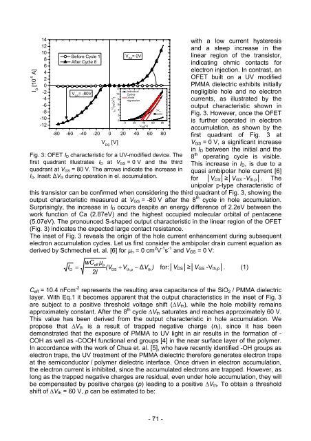
with a low current hysteresis<br />
and a steep increase in the<br />
linear region of the transistor,<br />
indicating ohmic contacts for<br />
electron injection. In contrast, an<br />
OFET built on a UV modified<br />
PMMA dielectric exhibits initially<br />
negligible hole and no electron<br />
currents, as illustrated by the<br />
output characteristic shown in<br />
Fig. 3. However, once the OFET<br />
is further operated in electron<br />
accumulation, as shown by the<br />
first quadrant of Fig. 3 at<br />
VGS = 0 V, a significant increase<br />
in ID between the initial and the<br />
8 th operating cycle is visible.<br />
This increase in ID, is due to a<br />
quasi ambipolar hole current [6]<br />
for │VDS│≥│VGS -Vth,p│. The<br />
unipolar p-type characteristic of<br />
this transistor can be confirmed when considering the third quadrant of Fig. 3, showing the<br />
output characteristic measured at VGS = -80 V after the 8 th cycle in hole accumulation.<br />
Surprisingly, the increase in ID occurs despite an energy difference of 2.2eV between the<br />
work function of Ca (2.87eV) and the highest occupied molecular orbital of pentacene<br />
(5.07eV). The pronounced S-shaped output characteristic in the linear region of the OFET<br />
(Fig. 3) indicates the expected large contact resistance.<br />
1/2 [10 -3 A 1/2 ]<br />
I D<br />
12<br />
10<br />
V DS [V]<br />
8<br />
6<br />
4<br />
2<br />
0<br />
V GS = 0V<br />
Individual<br />
Cycles<br />
Linear<br />
regression<br />
Fig. 3: OFET ID characteristic for a UV-modified device. The<br />
first quadrant illustrates ID at VGS = 0 V and the third<br />
quadrant at VGS = 80 V. The arrows indicate the increase in<br />
ID. Inset: ∆Vth during operation in el. accumulation.<br />
The inset of Fig. 3 reveals the origin of the hole current enhancement during subsequent<br />
electron accumulation cycles. Let us first consider the ambipolar drain current equation as<br />
derived by Schmechel et. al. [6] for µn = 0 cm 2 V -1 s -1 and VGS = 0 V:<br />
∆V th<br />
wCeff<br />
µ p<br />
= (VDS<br />
+ Vth,<br />
p − ∆V<br />
) for:│VDS│≥│VGS -Vth,p│. (1)<br />
2l<br />
ID th<br />
Ceff = 10.4 nFcm -2 represents the resulting area capacitance of the SiO2 / PMMA dielectric<br />
layer. With Eq.1 it becomes apparent that the output characteristics in the inset of Fig. 3<br />
are subject to a positive threshold voltage shift (∆Vth), while the hole mobility remains<br />
approximately constant. After the 8 th cycle ∆Vth saturates and reaches approximately 60 V.<br />
This value has been derived from the output characteristic in hole accumulation. We<br />
propose that ∆Vth is a result of trapped negative charge (nt), since it has been<br />
demonstrated that the exposure of PMMA to UV light in air results in the formation of -<br />
COH as well as -COOH functional end groups [4] in the near surface layer of the polymer.<br />
In accordance with the work of Chua et. al. [5], who have recently identified -OH groups as<br />
electron traps, the UV treatment of the PMMA dielectric therefore generates electron traps<br />
at the semiconductor / polymer dielectric interface. Once driven in electron accumulation,<br />
the electron current is inhibited, since the accumulated electrons are trapped. However, as<br />
long as the trapped negative charges are residual, even <strong>und</strong>er hole accumulation, they will<br />
be compensated by positive charges (p) leading to a positive ∆Vth. To obtain a threshold<br />
shift of ∆Vth = 60 V, p can be estimated to be:<br />
- 71 -