Electronic Material Properties - und Geowissenschaften ...
Electronic Material Properties - und Geowissenschaften ...
Electronic Material Properties - und Geowissenschaften ...
You also want an ePaper? Increase the reach of your titles
YUMPU automatically turns print PDFs into web optimized ePapers that Google loves.
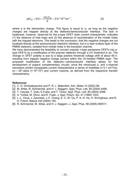
∆V<br />
C<br />
q<br />
th eff<br />
12 −2<br />
p ( VGS<br />
= 0V)<br />
= = 3.<br />
9 * 10 cm , (2)<br />
where q is the elementary charge. This figure is equal to nt, as long as the negative<br />
charges are trapped directly at the dielectric/semiconductor interface. The lack in<br />
hysteresis, however, observed for the p-type OFET drain current characteristic, indicates<br />
(1) the absence of hole traps and (2) the absence of recombination of the mobile holes<br />
with the trapped electrons. This leads to the conclusion, that the negative charges are not<br />
localized directly at the semiconductor dielectric interface, but in a near surface layer of the<br />
PMMA dielectric, isolated from mobile holes in the transistor channel.<br />
We have demonstrated the feasibility to convert unipolar n-type pentacene OFETs into ptype<br />
OFETs by a modification of the polymer dielectric through a UV treatment in air. The<br />
change in OFET polarity is due to a large positive threshold voltage shift of about 60 V,<br />
resulting from trapped negative charge carriers within the UV-treated PMMA layer. The<br />
proposed modification of the dielectric / semiconductor interface allows for the<br />
development of organic complementary circuits, since the introduced p- and n-channel<br />
transistors exhibit comparable current characteristics in terms of mobilities (≈ 0,1 cm 2 /Vs),<br />
on / off ratios (≈ 10 4 -10 5 ) and current maxima, as derived from the respective transfer<br />
characteristics.<br />
References<br />
[1] C. D. Dimitrakopoulos and P. R. L. Malenfant, Adv. Mater.14 (2002) 99.<br />
[2] M. Ahles, R. Schmechel, and H. v. Seggern, Appl. Phys. Lett. 85 (2004) 4499.<br />
[3] T. Yasuda, T. Goto, K.Fujita, and T. Tsutui, Appl. Phys. Lett. 85 (2004) 2098.<br />
[4] A. Torikai, M. Ohno, and K. Fueki, J. Appl. Polym. Sci. 41 (1990) 1023.<br />
[5] L.-L. Chua, J. Zaumseil, J.-F. Chang, E. C.-W. Ou, P. K.-H. Ho, H. Sirringhaus, and R.<br />
H. Friend, Nature 434 (2005) 194.<br />
[6] R. Schmechel, M. Ahles, and H. v. Seggern, J. Appl. Phys. 98 (2005) 084511.<br />
- 72 -


