

Electronic Material Properties - und Geowissenschaften ...
Electronic Material Properties - und Geowissenschaften ...
Electronic Material Properties - und Geowissenschaften ...

You also want an ePaper? Increase the reach of your titles
YUMPU automatically turns print PDFs into web optimized ePapers that Google loves.
In the XRD spectra, apart from the peaks of Ti and Ta, small peaks of the respective<br />
carbide phases MeC can be identified. Carbon implantation led to formation of the<br />
carbide phase. The peaks are rather weak and broad, which is assumed to be a<br />
consequence of small grain sizes and the shallowness of the implanted zone. XPS<br />
combined with Ar sputtering showed the development of the binding conditions with<br />
depth. In the C1s spectrum, on top of the sample, a thin film of elemental carbon was<br />
fo<strong>und</strong>. After 1 min sputtering, a chemical shift to carbide was detected. With<br />
increasing sputtering time, i.e. depth, the C signal became smaller and vanished,<br />
when the thickness of the implant region was exceeded. The Ti2p signal appeared at<br />
the position of the carbide and shifted to the position of elemental Ti upon sputtering.<br />
This showed that the TiC phase had been formed, in accordance with XRD.<br />
Basically, the same result was fo<strong>und</strong> for Ta in the C1s and Ta4f spectra.<br />
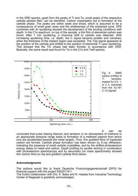
Fig. 4: SIMS<br />
carbon profiles of<br />
Ti samples,<br />
treated for 0.5, 1,<br />
or 2 h, extracted<br />
from the Ta-181<br />
C-12 signals<br />
It can be<br />
concluded that pulse biasing titanium and tantalum in an atmosphere of methane in<br />
an appropriate pressure range leads to formation of a methane plasma from which<br />
ions are accelerated towards the metal targets. Thus, thin gradient films of implanted<br />
carbon are formed. Carbide phase formation has been shown by X-ray diffraction,<br />
indicating the presence of small carbide crystallites, and by the shifted photoelectron<br />
energy states of metal and carbon. Depth profiling by sputter etching in combination<br />
with photoelectron spectroscopy and by secondary ion mass spectrometry showed<br />
thin carbon films on top and gradient carbide films below.<br />
Acknowledgments<br />
The authors would like to thank Deutsche Forschungsgemeinschaft (DFG) for<br />
financial support with the project EN207/19-1.<br />
The fruitful collaboration with Drs. K. Baba and R. Hatada from Industrial Technology<br />
Center of Nagasaki is gratefully acknowledged.<br />
- 91 -