

Electronic Material Properties - und Geowissenschaften ...
Electronic Material Properties - und Geowissenschaften ...
Electronic Material Properties - und Geowissenschaften ...

Create successful ePaper yourself
Turn your PDF publications into a flip-book with our unique Google optimized e-Paper software.
Alkyl- and aryl-modified Si(111) for silicon/organic hybrid devices<br />
Ralf Hunger, Wolfram Jaegermann<br />
Silicon/Organic junctions attract interest in several application perspectives: for<br />
silicon/organic hybrid devices such as biosensors, storage devices, or solar cells, as well<br />
as in the perspective of molecular electronics. It combines the advantages of modularity<br />
and tailoring capabilities of organic chemistry with the established, industrial-scale proven<br />
silicon technology.<br />
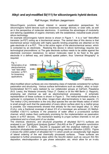
An example silicon/organic hybrid device is shown in Figure 1. It is a “wet” field-effect<br />
transistor (w-FET) acting as a biochemical sensor. The central idea of this device is that<br />
biochemical sensor molecules with highly specific binding properties are attached on the<br />
gate electrode of a w-FET. This is the active region of the electrochemical sensor, which<br />
is contacted by an electrolyte. Realizing this device in silicon technology requires two<br />
technological preconditions: a) The gate electrode surface needs to be stable against the<br />
electrolyte (corrosion resistance). b) sensor molecules need to be fixed to the gate<br />
electrode in a defined way, and (lateral) spatial pattern, thus “chemical lithography” is<br />
required.<br />
Fig. 1:<br />
Schematics of an<br />
electrochemical,<br />
“wet” field effect<br />
transistor, w-FET,<br />
for biosensing<br />
applications.<br />
Alkyl-modified silicon surfaces are one interesting class of materials considered for surface<br />
passivation and structuring. Various surface terminations such as methyl-, ethyl, or butylfunctionalized<br />
Si(111) were realized by our collaborator groups at CalTech, Pasadena<br />
(N.S. Lewis), the Waseda University Tokyo (T. Osaka) or at the HMI Berlin (J. Rappich),<br />
employing wet chemical as well as electrochemical processing. A schematic<br />
representation of these surfaces is shown in Figure 3. The methyl-terminated surface is<br />
particular in comparison to the other, longer-chain alkyl-terminations in two aspects: (1)<br />
The methyl (-CH3) termination is the only alkyl species the van-der-Waals radius of which<br />
is small enough such that the passivation of every silicon surface atom by a methyl group<br />
is possible. Our measurements showed that already for the next largest alkyl, i.e. ethyl<br />
(C2H5), only a fractional coverage of about 2/3 of a monolayer are achieved. (2) Methylmodified<br />
n-Si(111) surfaces in the presence of water affect a p-conductive surface<br />
channel, which makes them particularly promising for the implementation as passivation<br />
layers in w-FET devices. The mechanism leading to p-type surface channels is not yet<br />
<strong>und</strong>erstood and is a focal point of our studies.<br />
The chemical, electronic, and structural properties of alkylated Si(111) surfaces are<br />
analysed in our “Solid/Liquid Analysis System” (SoLiAS) at the 3 rd generation synchrotron<br />
facility BESSY II in Berlin. SoLiAS is equipped with the analytical methods of highresolution<br />
photoelectron spectroscopy and low energy electron diffraction (LEED). Figure<br />
2 shows the LEED pattern of ethylated Si(111) which proofs an exceptionally high degree<br />
of lateral ordering of the wet chemically processed surfaces. These surfaces are<br />
subjected to further processing steps within the SoLiAS station such as vacuum thin film<br />
deposition, electrodeposition or gas phase adsorption, etc. which allow for an in-situ<br />
- 75 -