

Electronic Material Properties - und Geowissenschaften ...
Electronic Material Properties - und Geowissenschaften ...
Electronic Material Properties - und Geowissenschaften ...

You also want an ePaper? Increase the reach of your titles
YUMPU automatically turns print PDFs into web optimized ePapers that Google loves.
Dielectric interface trap engineering by UV irradiation: A novel<br />
method to control OFET charge carrier transport properties<br />
N. Benson, M. Schidleja, C. Melzer, H. von Seggern<br />
For modern day electronics the integration of field effect transistors with complementary<br />
polarity on a single substrate is essential, in order to enhance the logic capability of the<br />
respective circuits. When considering organic electronics, however, this has proven<br />
difficult since most organic semiconductors exhibit either suitable hole (p) or electron (n)<br />
conduction [1]. The development of organic circuitry therefore requires the deposition of<br />
spatially separated p- and n-type organic semiconductors. However, recent publications<br />
[2,3] revealed the importance of the dielectric/semiconductor interface for charge carrier<br />
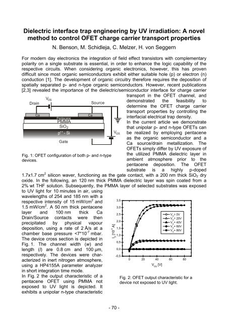
Drain<br />
Ca<br />
V DS<br />
Pentacene<br />
PMMA<br />
SiO2 ++ p - Si<br />
Gate<br />
Fig. 1: OFET configuration of both p- and n-type<br />
devices.<br />
Ca<br />
Source<br />
transport in the OFET channel, and<br />
demonstrated the feasibility to<br />
determine the OFET charge carrier<br />
transport properties by controlling the<br />
interfacial electrical trap density.<br />
In the current article we demonstrate<br />
that unipolar p- and n-type OFETs can<br />
be realized by employing pentacene<br />
as the organic semiconductor and a<br />
Ca source/drain metallization. The<br />
OFETs simply differ by UV exposure of<br />
the utilized PMMA dielectric layer in<br />
ambient atmosphere prior to the<br />
pentacene deposition. The OFET<br />
substrate is a highly p-doped<br />
1.7x1.7 cm 2 silicon waver, functioning as the gate contact, with a 200 nm thick SiO2 dry<br />
oxide. In the following, an 120 nm thick PMMA dielectric layer was spin coated from a<br />
2% wt THF solution. Subsequently, the PMMA layer of selected substrates was exposed<br />
to UV light for 10 minutes in air, using<br />
wavelengths of 254 and 185 nm with a<br />
respective intensity of 15 mW/cm 2 and<br />
1.5 mW/cm 2 . A 50 nm thick pentacene<br />
layer and 100 nm thick Ca<br />
Drain/Source contacts were then<br />
precipitated by physical vapour<br />
deposition, using a rate of 2 Å/s at a<br />
chamber base pressure