

Electronic Material Properties - und Geowissenschaften ...
Electronic Material Properties - und Geowissenschaften ...
Electronic Material Properties - und Geowissenschaften ...

You also want an ePaper? Increase the reach of your titles
YUMPU automatically turns print PDFs into web optimized ePapers that Google loves.
intensity I [a.u.]<br />
intensity I [a.u.]<br />
a)<br />
111<br />
200<br />
200<br />
220<br />
220<br />
311<br />
30 40 50 60 70 80 90 100 110 120<br />
b)<br />
111<br />
texture<br />
311<br />
texture<br />
30 40 50 60 70 80 90 100 110 120<br />
222<br />
222<br />
diffraction angle 2θ [°]<br />
400<br />
400<br />
331 420<br />
331 420<br />
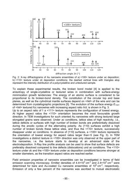
Fig. 2: X-ray diffractograms of Au nanowire ensembles of a) texture <strong>und</strong>er ac deposition;<br />
b) texture <strong>und</strong>er dc deposition conditions; the dashed vertical lines with triangles atop<br />
represent the intensity distribution of a polycrystalline and untextured sample.<br />
To explain these experimental results, the broken bond model [4] is applied to the<br />
anisotropy of single-crystalline or textured wires in combination with surface-energy<br />
minimization growth tendencies: The energy of an atomic surface is considered to be<br />
proportional to its broken-bond density. The constitution of the circular top and base<br />
planes, as well as the cylindrical mantle surfaces depend on of the wire and can be<br />
determined from crystallographic projections [5]. The evolution of the surface energy E<br />
of textured fcc nanowires with increasing aspect ratio h/d, is shown in Fig. 3.<br />
Up to an aspect ratio of 1 a texture represents the configuration of lowest energy.<br />
At higher aspect ratios the orientation becomes the most favourable growth<br />
direction. In TEM investigations for such oriented Au nanowires with strong textured large<br />
elongated grains were observed. Under ac conditions, lattice sites of high reactivity, i.e.,<br />
lattice defects or surfaces with high number of broken bonds are preferentially dissolved<br />
during the anodic cycles of the alternating polarity. As {110} surfaces exhibit a high<br />
number of broken bonds these lattice sites, and thus the texture, successively<br />
disappear <strong>und</strong>er ac conditions. In absence of {110} surfaces, a texture represents<br />
the orientation of lowest energy for aspect ratios larger than~5 (see Fig. 3). In TEM<br />
investigations a distinct texture in direction was only observed at the upper part of<br />
the nanowires, i.e. the texture starts to develop at an advanced state of the<br />
electrodeposition. X-Ray line profile analysis can be used to show that surface defects are<br />
preferably dissolved compared to line defects (dislocations) <strong>und</strong> ac conditions. The <br />
texture <strong>und</strong>er dc and the texture <strong>und</strong>er ac deposition conditions become stronger at<br />
smaller diameters, as the transition aspect ratios are reached earlier.<br />
Field emission properties of nanowire ensembles can be investigated in terms of field<br />
emission scanning microscopy. Emitter densities of 4.4×10 4 cm -2 and 2.4×10 4 cm -2 were<br />
determined for bare and Au-coated Cu nanowire ensembles of 10 6 cm -2 , respectively.<br />
Emission of only a few percent of the nanowires was ascribed to mutual electrostatic<br />
- 85 -