

Electronic Material Properties - und Geowissenschaften ...
Electronic Material Properties - und Geowissenschaften ...
Electronic Material Properties - und Geowissenschaften ...

Create successful ePaper yourself
Turn your PDF publications into a flip-book with our unique Google optimized e-Paper software.
Texture investigations and field emission properties<br />
of metallic nanowires<br />
Florian Maurer, Joachim Brötz, and Hartmut Fueß<br />
Due to their quasi one-dimensional geometry metallic nanowires possess high aspect<br />
ratios, i.e. high ratio of length over diameter. High nanowire aspect ratios, as well as small<br />
radii of curvature of the nanowire tips lead to an amplification of an externally applied<br />
electric field [1] and thus increases the probability of a field emission current by tunnelling.<br />
For field emission applications of vertically-aligned metallic nanowire ensembles it is<br />
desirable to control the aspect ratio, as well as the radius of curvature. A suitable method<br />
to fabricate high aspect nanowire ensembles (diameter a few ten nm, length a few ten µm)<br />
with controllable geometric and structural properties is the polymer template technique [2]:<br />
Nanoporous templates are produced by irradiating polymeric foils with accelerated heavy<br />
ions. After chemical etching of the ion-induced damage tracks, the cylindrical pores of the<br />
template are filled with metal by electrodeposition. The nanowire diameter is adjusted by<br />
the time of etching the ion-induced tracks and its height is controlled during<br />
electrodeposition by coulometry. The radius of curvature, i.e. the degree of single<br />
crystallinity can be controlled by different electrodeposition parameters, e.g. temperature<br />
or overvoltage. Different preferred growth orientations, i.e. textures, of the nanowires might<br />
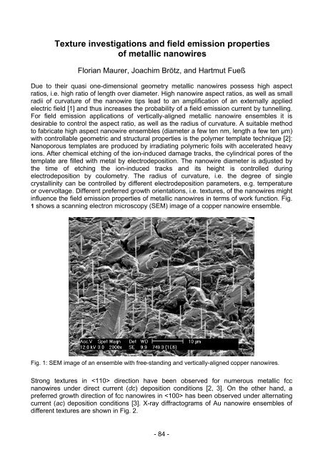
influence the field emission properties of metallic nanowires in terms of work function. Fig.<br />
1 shows a scanning electron microscopy (SEM) image of a copper nanowire ensemble.<br />
Fig. 1: SEM image of an ensemble with free-standing and vertically-aligned copper nanowires.<br />
Strong textures in direction have been observed for numerous metallic fcc<br />
nanowires <strong>und</strong>er direct current (dc) deposition conditions [2, 3]. On the other hand, a<br />
preferred growth direction of fcc nanowires in has been observed <strong>und</strong>er alternating<br />
current (ac) deposition conditions [3]. X-ray diffractograms of Au nanowire ensembles of<br />
different textures are shown in Fig. 2.<br />
- 84 -