

Electronic Material Properties - und Geowissenschaften ...
Electronic Material Properties - und Geowissenschaften ...
Electronic Material Properties - und Geowissenschaften ...

You also want an ePaper? Increase the reach of your titles
YUMPU automatically turns print PDFs into web optimized ePapers that Google loves.
Microstructure Characterization of Boron Suboxide, B6O<br />
Hans-Joachim Kleebe, Stefan Lauterbach, Mathias Herrmann 1 ,<br />
Jack Sigalas 2<br />
1 Fraunhofer Institut für Keramische Technologien <strong>und</strong> Systeme, Dresden<br />
2 University of the Witwatersrand, Johannesburg, Gauteng, South Africa<br />
Hexaboron monoxide (B6O), commonly termed boron suboxide, is known as a<br />
superhard material, constituted of the light elements boron and oxygen. The<br />
extraordinary hardness of such a low-density material has been attributed to the intrinsic<br />
strong and directional covalent bonds between B and O, leading to a tight, threedimensional<br />
network with an excellent resistance towards external shear.<br />
The average Vickers hardness (Hv) of B6O is about 45 GPa, which is next to diamond<br />
(Hv: 70–100 GPa) and cubic boron nitride, c-BN (Hv: 45–50 GPa). Similarly, the<br />
average fracture toughness of B6O (4.5 MPa m 1/2 ) is higher as compared to c-BN (2.8<br />
MPa m 1/2 ) and comparable to diamond (5.0 MPa m 1/2 ). Due to its strong covalent<br />
bonding, B6O materials demonstrate exceptional physical and chemical performance<br />
such as high hardness, low density, high thermal conductivity, chemical inertness and<br />
good wear resistance. Its thermal stability, even at temperatures above 1000 °C, and<br />
its chemical inertness with ferrous alloys makes it in some instances even more suitable<br />
for industrial applications as for example diamond. In general, B6O materials have<br />
potential applications as abrasives, due to their high hardness, and are also considered<br />
as potential candidates for high-temperature semiconductors (with an estimated band<br />
gap of approximately 2.4 eV) and for<br />
thermo-electrics. Despite various potential<br />
applications, densification and processing<br />
of B6O materials was shown to be rather<br />
cumbersome. Therefore, a detailed<br />
microstructure characterization was<br />
performed in order to gain insight in the<br />
submicron structure that formed upon<br />
sintering.<br />
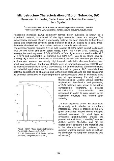
ACerS – NIST Phase Equilibria Diagrams<br />
Fig. 02339—System Al2O3-B2O3.<br />
P. J. M. Gielisse and W. R. Foster, Nature<br />
(London), 195 [4836] 69-70 (1962).<br />
The main objectives of the TEM study were<br />
(i) to verify as to whether an amorphous<br />
intergranular phase is present at the B6O<br />
grain bo<strong>und</strong>aries (doped versus <strong>und</strong>oped<br />
sintered samples), (ii) what type of<br />
crystalline grain-bo<strong>und</strong>ary phases are<br />
present in the sintered, coated B6O sample:<br />
Al4B2O9 and/or Al18B4O33, and (iii) the<br />
overall defect structure in the materials was<br />
to be characterized (in particular, the<br />
question whether stacking faults in B6O can<br />
be eliminated via long-term annealing was<br />
addressed).<br />
- 153 -