

Electronic Material Properties - und Geowissenschaften ...
Electronic Material Properties - und Geowissenschaften ...
Electronic Material Properties - und Geowissenschaften ...

Create successful ePaper yourself
Turn your PDF publications into a flip-book with our unique Google optimized e-Paper software.
Breakdown-induced light emission and poling dynamics of<br />
porous fluoropolymers<br />
S. Zhukov and H. von Seggern<br />
Recently, a new class of plastics with a very strong piezoelectricity has been discussed in<br />
literature: foams. It has been demonstrated that inner pores, when properly charged in an<br />
external electric field, are responsible for a high piezoelectric response of cellular<br />
polypropylene (PP) [1-3] and expanded polytetrafluoroethylene (ePTFE) [3-5] films.<br />
Surprisingly, a strong difference in the obtainable polarization and the related piezoelectric<br />
d33 coefficients has been recognized between samples with closed-pore (PP) and openpore<br />
(ePTFE) geometry. Most research groups report quasi-static or low-frequency<br />
dynamic coefficients up to 200 pC/N on standard grades of porous PP films, whereas the<br />
open-porous ePTFE films reveal rather small values of 10 to 20 pC/N.<br />
Up to date the charging mechanism of open-porous electrets materials is not completely<br />
<strong>und</strong>erstood. To clarify this issue, we investigated the emission of light during the corona<br />
poling of single ePTFE films and the same film sandwiched between two solid FEP films.<br />
Generally, the charging mechanism is supposed to arise from electrical breakdown within<br />
the voids during the poling process [4,5]. The separation of charges due to the electrical<br />
breakdown leads to the aspired polarization buildup. However, each breakdown event is<br />
accompanied by light emission. Thus the emission of light can be considered as a direct<br />
proof of the occurrence of breakdown events and indicates an ongoing poling process<br />
within the sample.<br />
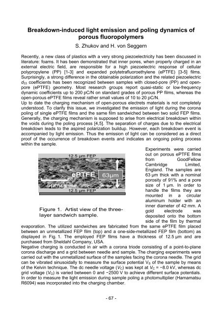
Experiments were carried<br />
12.5 µm FEP<br />
ePTFE<br />
5µm 12.5 µm FEP<br />
out on porous ePTFE films<br />
from GoodFellow<br />
Cambridge Limited,<br />
England. The samples are<br />
63 µm thick with a nominal<br />
porosity of 91% and a pore<br />
size of 1 µm. In order to<br />
handle the films they are<br />
mounted in a circular<br />
aluminum holder with an<br />
inner diameter of 42 mm. A<br />
gold electrode was<br />
deposited onto the bottom<br />
side of the film by thermal<br />
evaporation. The utilized sandwiches are fabricated from the same ePTFE film placed<br />
between an unmetallized FEP film (top) and a one-side-metallized FEP film (bottom) as<br />
displayed in Fig. 1. The employed FEP films have a thickness of 12.5 µm and are<br />
purchased from Sheldahl Company, USA.<br />
63µm<br />
Figure 1. Artist view of the threelayer<br />
sandwich sample.<br />
Negative charging is conducted in air with a corona triode consisting of a point-to-plane<br />
corona discharge and a grid between needle and sample. The charging experiments were<br />
carried out with the unmetallized surface of the samples facing the corona needle. The grid<br />
can be vibrated sinusoidally to measure the surface potential VS of the sample by means<br />
of the Kelvin technique. The dc needle voltage (VC) was kept at VC = −8.0 kV, whereas dc<br />
grid voltage (VG) is varied between 0 and −2500 V to achieve different surface potentials.<br />
In order to measure the light emission during sample poling a photomultiplier (Hamamatsu<br />
R6094) was incorporated into the charging chamber.<br />
- 67 -