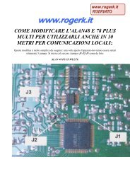
- Page 1 and 2:
Modifications for the ICOMcreated 2
- Page 3 and 4:
(IC-271)(IC-271)(IC-271)(IC-2710)(I
- Page 5 and 6:
(IC-475)(IC-475)(IC-475)(IC-475)(IC
- Page 7 and 8:
(IC-756pro) Expand tx-freqeuncy for
- Page 9 and 10:
(IC-W2E)(IC-W31)(IC-W31)(IC-W31)(IC
- Page 11 and 12:
2. After about 0.5 second, press st
- Page 13 and 14:
21-10-1999(AT-500) ICOM AT-500 Tune
- Page 15 and 16:
4. Program the radio to the local w
- Page 17 and 18:
19-07-1998(IC-03) ICOM 02/03/04 & V
- Page 19 and 20:
This modification is read 553 times
- Page 21 and 22:
6. Reinstall the RAM board into the
- Page 23 and 24:
27-10-1998(IC-1275) Power control m
- Page 25 and 26:
27-10-1998(IC-1275) Modification of
- Page 27 and 28:
●Connect the short plug end with
- Page 29 and 30:
This modification is read 1316 time
- Page 31 and 32:
50MHz to something like 204MHz cont
- Page 33 and 34:
26-07-2001(IC-207) Band Expansion f
- Page 35 and 36:
This modification is read 4219 time
- Page 37 and 38:
Fig. 3: The circuit extract from IC
- Page 39 and 40:
19-07-1998(IC-22) Icom IC22S Packet
- Page 41 and 42:
This modification is read 739 times
- Page 43 and 44:
More detailed:In the true spirit of
- Page 45 and 46:
19-07-1998(IC-229) IC-229H Fix CPU/
- Page 47 and 48:
In addition, if you want to put an
- Page 49 and 50:
By diode:●●Remove D17 diode on
- Page 51 and 52:
1. Remove diode D14 (if there is an
- Page 53 and 54:
cut... I'm guessing, but it could b
- Page 55 and 56:
19-07-1998(IC-24) IC-24AT enabling
- Page 57 and 58:
19-07-1998(IC-24) Tip to to functio
- Page 59 and 60:
This complete the mods done with su
- Page 61 and 62:
This modification is read 726 times
- Page 63 and 64:
Comment:These TRX is accorded to my
- Page 65 and 66:
this mod of use as I have.Any comme
- Page 67 and 68:
other wires come in. Take the cable
- Page 69 and 70:
17-11-2000(IC-2700) Enabling ICOM 2
- Page 71 and 72:
19-07-1998(IC-271) IC-271 / 471 fue
- Page 73 and 74:
RAM card version B images:This modi
- Page 75 and 76:
12-11-2000(IC-2710) Crossband Repea
- Page 77 and 78:
Note:From Bill K7RIEICOM has not tr
- Page 79 and 80:
19-07-1998(IC-275) Improve the stab
- Page 81 and 82:
●●●●●●●●●●remov
- Page 83 and 84:
Note: a strong signal will be serio
- Page 85 and 86:
19-07-1998(IC-28) The long, noisy s
- Page 87 and 88:
not a hard mod to do,..........but
- Page 89 and 90:
02-04-2000(IC-2800) IC-2800H cross
- Page 91 and 92:
19-07-1998(IC-281) Extended Receive
- Page 93 and 94: encased it in shrink-tube. The oper
- Page 95 and 96: push buttonswitch ^ ^| |___________
- Page 97 and 98: 19-07-1998(IC-2IA) IC-2IA lousey xm
- Page 99 and 100: 1. Change to RECEIVER MODE (not rec
- Page 101 and 102: 13.0V 5.0W12.0V 5.0W11.0V 5.0W10.0V
- Page 103 and 104: This modification is read 748 times
- Page 105 and 106: MODIFICATION (Refer to figure 1.)1.
- Page 107 and 108: Procedure1. Remove the covers from
- Page 109 and 110: 19-07-1998(IC-3200) Fix for IC-3200
- Page 111 and 112: 4. select a frequency of 150.000Mhz
- Page 113 and 114: 19-07-1998(IC-3220) How to iface Ic
- Page 115 and 116: Now power on and type in the freque
- Page 117 and 118: One note on the above - the BNC con
- Page 119 and 120: e shorted to ground and cause PLL u
- Page 121 and 122: 19-07-1998(IC-451) IC-451 aus 9600F
- Page 123 and 124: 3. If by accident you lose power to
- Page 125 and 126: 19-07-1998(IC-475) IC-475 Freq. ste
- Page 127 and 128: Problem:This is a general transceiv
- Page 129 and 130: Note: a strong signal will be serio
- Page 131 and 132: Das spart einen mords Haufen Arbeit
- Page 133 and 134: Dieses ist mit dieser Schaltung als
- Page 135 and 136: This modification is read 565 times
- Page 137 and 138: X . X . 5.0 KHz 1 0 1 0. . . . X .
- Page 139 and 140: Remove the back cover. If you place
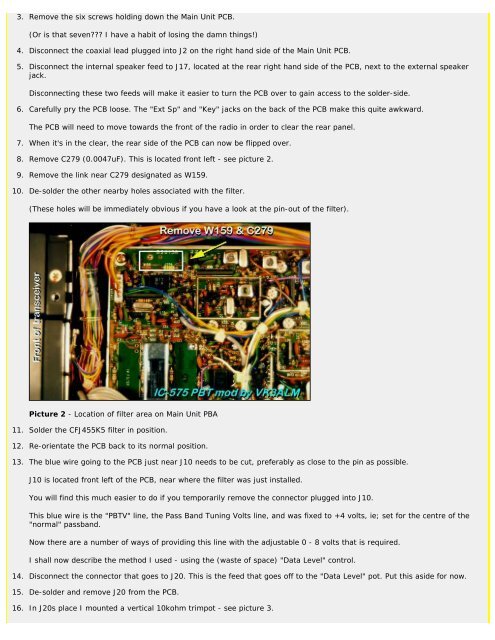
- Page 141 and 142: 27-10-1998(IC-575) SSB RF GainProbl
- Page 143: 26-06-2001(IC-575) Pass band Tuning
- Page 147 and 148: 19-07-1998(IC-706) Info/mods for IC
- Page 149 and 150: ¦ ¦¦ ¦¦ ¦¦ ¦¦ ¦----------
- Page 151: ●●●●●●●●●●●
- Page 154 and 155: From: gary@ke4zv.atl.ga.us (Gary Co
- Page 156 and 157: Mehr Dynamik in der Modulation beko
- Page 158 and 159: Operation:Be sure to read the manua
- Page 160 and 161: Alternative zum modifizierten PC St
- Page 162 and 163: ●●●●●(Another receiver wi
- Page 164 and 165: | IC31 uPD4094BG || |1 2 3 4 |5 6 7
- Page 166 and 167: This modification is read 411 times
- Page 168 and 169: D116 and D118 are responsible for o
- Page 170 and 171: Transmit power output after modific
- Page 172 and 173: This information and photos was sup
- Page 174 and 175: 22-02-2002(IC-706MKII) IC-706MKIIG
- Page 176 and 177: This modification is read 2320 time
- Page 178 and 179: Delete cap. CT14 at pin 6 of IC3 on
- Page 180 and 181: 18-06-2000(IC-729) Using two Icom r
- Page 182 and 183: 19-07-1998(IC-735) IC-735 Remote Wo
- Page 184 and 185: 19-07-1998(IC-736) Icom IC-736 DDS/
- Page 186 and 187: Also probably would apply to IC 735
- Page 188 and 189: RAM card version B images:This modi
- Page 190 and 191: John Schmitz NS8EAdditional informa
- Page 192 and 193: 13-01-2002(IC-746) Monitor Audio Ou
- Page 194 and 195:
This modification is read 1499 time
- Page 196 and 197:
19-07-1998(IC-751) IC-751 Bad Cap P
- Page 198 and 199:
inspect your job to be sure that th
- Page 200 and 201:
28-01-2002(IC-751) ICOM IC-751 Dual
- Page 202 and 203:
Step 8: Turn the radio off and inst
- Page 204 and 205:
To be neater you could remove the s
- Page 206 and 207:
[W804] | |Remove=>[W805] | CHIP |[W
- Page 208 and 209:
Date: 23-02-2002 User comment From:
- Page 210 and 211:
less.The second way to adjust the I
- Page 212 and 213:
23-11-2001(IC-756pro2) IC-756PRO2 T
- Page 214 and 215:
19-07-1998(IC-765) Icom IC-765 Pass
- Page 216 and 217:
19-07-1998(IC-775) New product info
- Page 218 and 219:
70% AM.My personal findings are tha
- Page 220 and 221:
11. Re-install board and all cables
- Page 222 and 223:
The Yaesu FT726R first appeared ten
- Page 224 and 225:
There seemed to be no way of changi
- Page 226 and 227:
Add a diode on the blank position b
- Page 228 and 229:
---- gar keine Diode ----Breitband
- Page 230 and 231:
To disable the x-band repeater just
- Page 232 and 233:
Well this should make things verry
- Page 234 and 235:
Set radio in VFO mode, and select f
- Page 236 and 237:
27-05-2001(IC-910) Expanded functio
- Page 238 and 239:
●●●350-470 MHz RX/TX800-950 M
- Page 240 and 241:
This modification is read 242 times
- Page 242 and 243:
This modification is read 270 times
- Page 244 and 245:
1. You're completely successful.2.
- Page 246 and 247:
●●●●●●●●●Für Han
- Page 248:
28-03-1999(IC-Q7) Modifying the ICO
- Page 252 and 253:
●●●●●●●●Desoldering
- Page 254 and 255:
You should now have the RF board co
- Page 256 and 257:
This modification is read 2358 time
- Page 258 and 259:
BOOT:Attenuator protecs strong sign
- Page 260 and 261:
1. Use an ohmmeter to determine whi
- Page 262 and 263:
2. Remove battery cover and battery
- Page 264 and 265:
Fig. 4. Receiving AO-40 (at MA=13)O
- Page 266 and 267:
This modification can also be found
- Page 268 and 269:
The Q and not Q outputs on this IC
- Page 270 and 271:
Date: 30-12-2001 User comment From:
- Page 272 and 273:
This modification is read 3462 time
- Page 274 and 275:
Removing 1F unit1. Pull the 2 knobs
- Page 276 and 277:
16-05-1999(IC-T8) Problem with the
- Page 278 and 279:
800 -
- Page 280 and 281:
Frequencyrange after modification:5
- Page 282 and 283:
Offset Freq: Hold [FUNC], Press [4]
- Page 284 and 285:
This modification is read 866 times
- Page 286 and 287:
The Icom IC W21AT handi-talkie norm
- Page 288 and 289:
19-07-1998(IC-W2A) IC-W2A signal le
- Page 290 and 291:
19-07-1998(IC-W31) IC-W31E CROSS-BA
- Page 292 and 293:
15-10-2000(IC-W31) Cross Band Repea
- Page 294 and 295:
could always try it.Set VHF and UHF
- Page 296 and 297:
31-07-2001(IC-W32) Icom IC-W32A pro
- Page 298 and 299:
This modification is read 697 times
- Page 300 and 301:
This modification is read 580 times
- Page 302 and 303:
IC-4GAT - Turn the radio on, hold [
- Page 304 and 305:
IC-M9 - Hold [HI/LO] & [DW/SCAN] bu
- Page 306 and 307:
IC-275H 10IC-375A 12IC-471 22IC-475
- Page 308 and 309:
I have tested this mod with a ic-75
- Page 310 and 311:
How further up the hole is the bett
- Page 312 and 313:
Connect the NTC, FAN and power and
- Page 314 and 315:
5, 31, 48, and 79.4. Does the Prior
- Page 316 and 317:
19-07-1998(R-7000) Modify your ICOM
- Page 318 and 319:
1. C231 from 1000 pf to 68 pf.2. C2
- Page 320 and 321:
This modification is read 741 times
- Page 322 and 323:
This modification is read 877 times
- Page 324 and 325:
19-07-1998(R-71) Tricking the ICOM
- Page 326 and 327:
There are two wires which send logi
- Page 328 and 329:
A. Remove the top cover of the rece
- Page 330 and 331:
08-11-1998(R-7100) Modify your Icom
- Page 332 and 333:
17-03-2002(R-7100) Icom R7100 Discr
- Page 334:
23-08-1998(R-8500) Operating the Ic