TMS320VC5409 Fixed-Point Digital Signal ... - Texas Instruments
TMS320VC5409 Fixed-Point Digital Signal ... - Texas Instruments
TMS320VC5409 Fixed-Point Digital Signal ... - Texas Instruments
- No tags were found...

You also want an ePaper? Increase the reach of your titles
YUMPU automatically turns print PDFs into web optimized ePapers that Google loves.
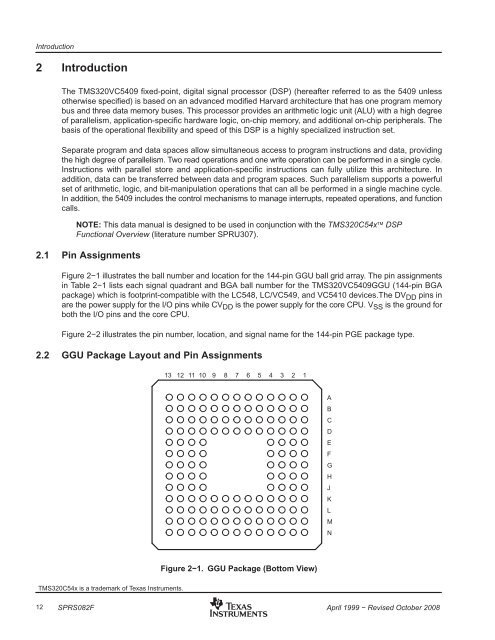
Introduction2 IntroductionThe <strong>TMS320VC5409</strong> fixed-point, digital signal processor (DSP) (hereafter referred to as the 5409 unlessotherwise specified) is based on an advanced modified Harvard architecture that has one program memorybus and three data memory buses. This processor provides an arithmetic logic unit (ALU) with a high degreeof parallelism, application-specific hardware logic, on-chip memory, and additional on-chip peripherals. Thebasis of the operational flexibility and speed of this DSP is a highly specialized instruction set.Separate program and data spaces allow simultaneous access to program instructions and data, providingthe high degree of parallelism. Two read operations and one write operation can be performed in a single cycle.Instructions with parallel store and application-specific instructions can fully utilize this architecture. Inaddition, data can be transferred between data and program spaces. Such parallelism supports a powerfulset of arithmetic, logic, and bit-manipulation operations that can all be performed in a single machine cycle.In addition, the 5409 includes the control mechanisms to manage interrupts, repeated operations, and functioncalls.NOTE: This data manual is designed to be used in conjunction with the TMS320C54x DSPFunctional Overview (literature number SPRU307).2.1 Pin AssignmentsFigure 2−1 illustrates the ball number and location for the 144-pin GGU ball grid array. The pin assignmentsin Table 2−1 lists each signal quadrant and BGA ball number for the <strong>TMS320VC5409</strong>GGU (144-pin BGApackage) which is footprint-compatible with the LC548, LC/VC549, and VC5410 devices.The DV DD pins inare the power supply for the I/O pins while CV DD is the power supply for the core CPU. V SS is the ground forboth the I/O pins and the core CPU.Figure 2−2 illustrates the pin number, location, and signal name for the 144-pin PGE package type.2.2 GGU Package Layout and Pin Assignments13 12 11 10 987654321ABCDEFGHJKLMNFigure 2−1. GGU Package (Bottom View)TMS320C54x is a trademark of <strong>Texas</strong> <strong>Instruments</strong>.12 SPRS082FApril 1999 − Revised October 2008