TMS320VC5409 Fixed-Point Digital Signal ... - Texas Instruments
TMS320VC5409 Fixed-Point Digital Signal ... - Texas Instruments
TMS320VC5409 Fixed-Point Digital Signal ... - Texas Instruments
- No tags were found...

You also want an ePaper? Increase the reach of your titles
YUMPU automatically turns print PDFs into web optimized ePapers that Google loves.
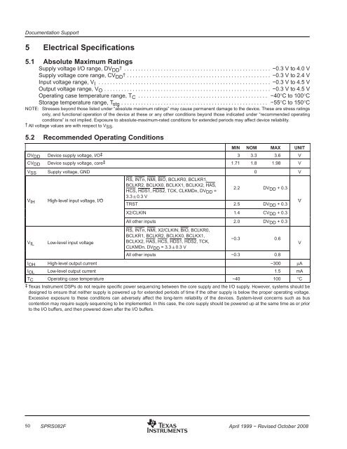
Documentation Support5 Electrical Specifications5.1 Absolute Maximum RatingsSupply voltage I/O range, DV DD† . . . . . . . . . . . . . . . . . . . . . . . . . . . . . . . . . . . . . . . . . . . . . . . . . . . . −0.3 V to 4.0 VSupply voltage core range, CV DD† . . . . . . . . . . . . . . . . . . . . . . . . . . . . . . . . . . . . . . . . . . . . . . . . . . . −0.3 V to 2.4 VInput voltage range, V I . . . . . . . . . . . . . . . . . . . . . . . . . . . . . . . . . . . . . . . . . . . . . . . . . . . . . . . . . . . . . −0.3 V to 4.5 VOutput voltage range, V O . . . . . . . . . . . . . . . . . . . . . . . . . . . . . . . . . . . . . . . . . . . . . . . . . . . . . . . . . . . −0.3 V to 4.5 VOperating case temperature range, T C . . . . . . . . . . . . . . . . . . . . . . . . . . . . . . . . . . . . . . . . . . . . . . −40°C to 100°CStorage temperature range, T stg . . . . . . . . . . . . . . . . . . . . . . . . . . . . . . . . . . . . . . . . . . . . . . . . . . . . −55°C to 150°CNOTE: Stresses beyond those listed under “absolute maximum ratings” may cause permanent damage to the device. These are stress ratingsonly, and functional operation of the device at these or any other conditions beyond those indicated under “recommended operatingconditions” is not implied. Exposure to absolute-maximum-rated conditions for extended periods may affect device reliability.† All voltage values are with respect to VSS.5.2 Recommended Operating ConditionsMIN NOM MAX UNITDVDD Device supply voltage, I/O‡ 3 3.3 3.6 VCVDD Device supply voltage, core‡ 1.71 1.8 1.98 VVSS Supply voltage, GND 0 VVIHVILHigh-level input voltage, I/OLow-level input voltageRS, INTn, NMI, BIO, BCLKR0, BCLKR1,BCLKR2, BCLKX0, BCLKX1, BCLKX2, HAS,HCS, HDS1, HDS2, TCK, CLKMDn, DVDD =3.30.3 V2.2 DVDD + 0.3TRST 2.5 DVDD + 0.3X2/CLKIN 1.4 CVDD + 0.3All other inputs 2.0 DVDD + 0.3RS, INTn, NMI, X2/CLKIN, BIO, BCLKR0,BCLKR1, BCLKR2, BCLKX0, BCLKX1,BCLKX2, HAS, HCS, HDS1, HDS2, TCK,CLKMDn, DVDD = 3.30.3 V−0.3 0.6All other inputs −0.3 0.8IOH High-level output current −300 µAIOL Low-level output current 1.5 mATC Operating case temperature −40 100 °C‡ <strong>Texas</strong> Instrument DSPs do not require specific power sequencing between the core supply and the I/O supply. However, systems should bedesigned to ensure that neither supply is powered up for extended periods of time if the other supply is below the proper operating voltage.Excessive exposure to these conditions can adversely affect the long-term reliability of the devices. System-level concerns such as buscontention may require supply sequencing to be implemented. In this case, the core supply should be powered up at the same time as or priorto the I/O buffers, and then powered down after the I/O buffers.VV50 SPRS082FApril 1999 − Revised October 2008