TMS320VC5409 Fixed-Point Digital Signal ... - Texas Instruments
TMS320VC5409 Fixed-Point Digital Signal ... - Texas Instruments
TMS320VC5409 Fixed-Point Digital Signal ... - Texas Instruments
- No tags were found...

Create successful ePaper yourself
Turn your PDF publications into a flip-book with our unique Google optimized e-Paper software.
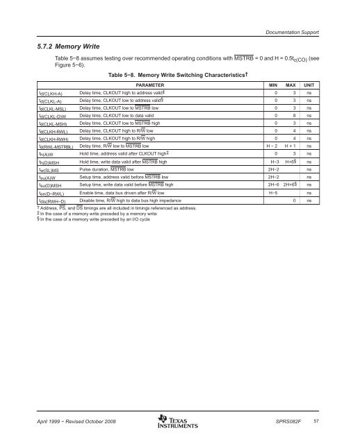
Documentation Support5.7.2 Memory WriteTable 5−8 assumes testing over recommended operating conditions with MSTRB = 0 and H = 0.5t c(CO) (seeFigure 5−6).Table 5−8. Memory Write Switching Characteristics †PARAMETER MIN MAX UNITtd(CLKH-A) Delay time, CLKOUT high to address valid‡ 0 3 nstd(CLKL-A) Delay time, CLKOUT low to address valid§ 0 3 nstd(CLKL-MSL) Delay time, CLKOUT low to MSTRB low 0 3 nstd(CLKL-D)W Delay time, CLKOUT low to data valid 0 8 nstd(CLKL-MSH) Delay time, CLKOUT low to MSTRB high 0 3 nstd(CLKH-RWL) Delay time, CLKOUT high to R/W low 0 4 nstd(CLKH-RWH) Delay time, CLKOUT high to R/W high 0 4 nstd(RWL-MSTRBL) Delay time, R/W low to MSTRB low H − 2 H + 1 nsth(A)W Hold time, address valid after CLKOUT high‡ 0 3 nsth(D)MSH Hold time, write data valid after MSTRB high H−3 H+6§ nstw(SL)MS Pulse duration, MSTRB low 2H−2 nstsu(A)W Setup time, address valid before MSTRB low 2H−2 nstsu(D)MSH Setup time, write data valid before MSTRB high 2H−6 2H+6§ nsten(D−RWL) Enable time, data bus driven after R/W low H−5 nstdis(RWH−D) Disable time, R/W high to data bus high impedance 0 ns† Address, PS, and DS timings are all included in timings referenced as address.‡ In the case of a memory write preceded by a memory write§ In the case of a memory write preceded by an I/O cycleApril 1999 − Revised October 2008SPRS082F57