TMS320VC5409 Fixed-Point Digital Signal ... - Texas Instruments
TMS320VC5409 Fixed-Point Digital Signal ... - Texas Instruments
TMS320VC5409 Fixed-Point Digital Signal ... - Texas Instruments
- No tags were found...

Create successful ePaper yourself
Turn your PDF publications into a flip-book with our unique Google optimized e-Paper software.
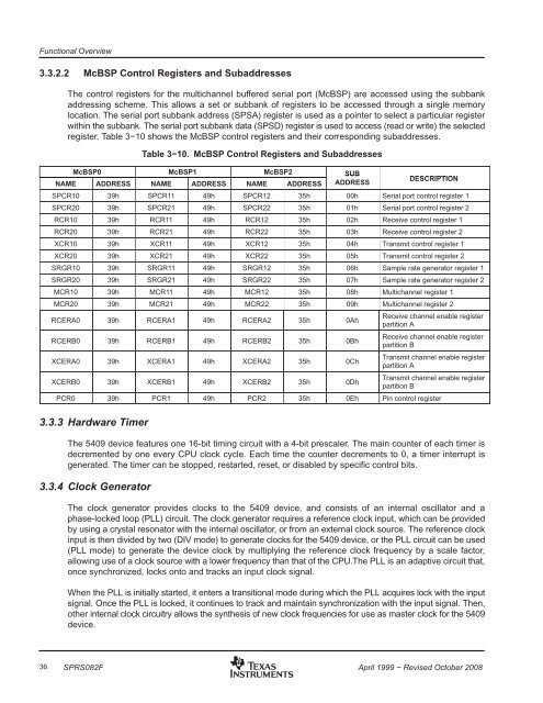
Functional Overview3.3.2.2 McBSP Control Registers and SubaddressesThe control registers for the multichannel buffered serial port (McBSP) are accessed using the subbankaddressing scheme. This allows a set or subbank of registers to be accessed through a single memorylocation. The serial port subbank address (SPSA) register is used as a pointer to select a particular registerwithin the subbank. The serial port subbank data (SPSD) register is used to access (read or write) the selectedregister. Table 3−10 shows the McBSP control registers and their corresponding subaddresses.Table 3−10. McBSP Control Registers and SubaddressesMcBSP0 McBSP1 McBSP2 SUBNAME ADDRESS NAME ADDRESSÁÁÁÁÁÁÁÁNAMEÁÁÁÁADDRESSÁÁÁÁÁÁÁÁADDRESSSPCR1039hSPCR1149h SPCR12 35h00hSPCR20 39h SPCR21 ÁÁÁÁÁ49h SPCR22 01hÁÁÁÁÁÁÁÁÁÁÁÁÁÁÁÁRCR10 ÁÁÁÁ39h RCR11 ÁÁÁÁÁ49h RCR12 ÁÁÁÁ02hÁÁÁÁÁÁÁÁRCR20 ÁÁÁÁ39h ÁÁÁÁÁRCR21 ÁÁÁÁ 49h ÁÁÁÁÁRCR22 ÁÁÁÁ 03hXCR10 ÁÁÁÁ39h ÁÁÁÁÁXCR11 ÁÁÁÁ 49h ÁÁÁÁÁXCR12 ÁÁÁÁ 04hXCR20 ÁÁÁÁ39h ÁÁÁÁÁXCR21 ÁÁÁÁ 49h ÁÁÁÁÁXCR22 ÁÁÁÁ 05hSRGR10 ÁÁÁÁ39h ÁÁÁÁÁSRGR11 ÁÁÁÁ 49h ÁÁÁÁÁSRGR12 ÁÁÁÁ 06hSRGR20 39h SRGR21 49h SRGR22 07hÁÁÁÁÁÁÁÁÁÁÁÁÁÁÁÁÁÁÁÁMCR10 39h MCR11 49h MCR12 35h08hMCR20 MCR21 MCR22 09hÁÁÁÁÁÁÁÁÁÁÁÁÁÁÁÁÁÁÁÁÁÁÁÁÁÁÁÁÁÁÁÁÁÁÁÁÁÁÁÁÁÁÁÁÁÁÁÁÁÁÁÁDESCRIPTIONSerial port control register 1ÁÁÁÁÁÁÁÁÁÁÁÁÁ35h ÁÁÁÁÁÁÁÁÁÁÁÁÁÁSerial port control register 235h ÁÁÁÁÁÁÁÁÁÁÁÁÁÁReceive control register 135h ÁÁÁÁÁÁÁÁÁÁÁÁÁÁReceive control register 235h ÁÁÁÁÁÁÁÁÁÁÁÁÁÁTransmit control register 135h ÁÁÁÁÁÁÁÁÁÁÁÁÁÁTransmit control register 235h ÁÁÁÁÁÁÁÁÁÁÁÁÁÁSample rate generator register 135h Sample rate generator register 2ÁÁÁÁÁÁÁÁÁÁÁÁÁMultichannel register 1ÁÁÁÁ ÁÁÁÁ ÁÁÁÁ39h 49h 35h ÁÁÁÁÁ ÁÁÁÁÁÁÁÁÁMultichannelÁÁÁÁÁregister 2ÁÁÁÁÁ ÁÁÁÁÁÁÁÁÁÁÁÁÁÁÁÁÁÁÁÁÁÁÁÁÁÁÁÁÁÁÁÁÁÁÁÁÁÁÁRCERA039hRCERA149hRCERA2ÁÁÁÁÁ ÁÁÁÁÁÁÁÁÁÁÁÁÁÁÁÁÁÁÁÁÁÁÁÁÁÁÁÁÁÁÁÁÁÁÁÁÁÁÁÁÁÁÁ 39h ÁÁÁÁÁ 49h ÁÁÁÁÁ 35h ÁÁÁÁÁ0Bh ÁÁÁÁÁÁÁÁÁÁÁÁÁÁÁÁÁRCERB0ÁÁÁÁXCERA0 39hRCERB1ÁÁÁÁXCERA1 49h35hRCERB2ÁÁÁÁXCERA2 35h0AhReceive channel enable registerpartition AReceive channel enable registerpartition BTransmit channel enable registerpartition ATransmit channel enable registerpartition BPin control registerÁÁÁÁÁÁÁÁÁÁÁÁÁÁÁÁÁÁÁÁÁÁÁÁÁÁÁÁÁÁÁÁÁÁÁÁÁÁÁÁÁÁÁÁÁÁÁÁÁÁÁÁÁÁÁÁÁÁÁÁÁÁÁÁÁÁÁÁÁÁÁÁÁÁÁÁÁÁÁÁÁÁÁÁÁÁÁÁÁ 39h ÁÁÁÁÁ 49h ÁÁÁÁÁXCERB2ÁÁÁÁ 35h ÁÁÁÁÁ0Dh ÁÁÁÁÁÁÁÁÁXCERB0 ÁÁÁÁPCR0XCERB1 ÁÁÁÁ39h PCR1ÁÁÁÁÁ49h PCR2ÁÁÁÁÁ0Ch35h 0EhÁÁÁÁÁÁÁÁÁÁÁÁÁÁÁÁÁÁÁÁÁÁÁÁÁ ÁÁÁÁ ÁÁÁÁ ÁÁÁÁ ÁÁÁÁÁÁÁÁÁ3.3.3 Hardware TimerÁÁÁÁÁÁÁÁÁÁÁÁÁÁÁÁÁÁÁÁÁÁÁÁÁÁÁÁÁÁÁÁÁÁÁThe 5409 device features one 16-bit timing circuit with a 4-bit prescaler. The main counter of each timer isdecremented by one every CPU clock cycle. Each time the counter decrements to 0, a timer interrupt isgenerated. The timer can be stopped, restarted, reset, or disabled by specific control bits.3.3.4 Clock GeneratorThe clock generator provides clocks to the 5409 device, and consists of an internal oscillator and aphase-locked loop (PLL) circuit. The clock generator requires a reference clock input, which can be providedby using a crystal resonator with the internal oscillator, or from an external clock source. The reference clockinput is then divided by two (DIV mode) to generate clocks for the 5409 device, or the PLL circuit can be used(PLL mode) to generate the device clock by multiplying the reference clock frequency by a scale factor,allowing use of a clock source with a lower frequency than that of the CPU.The PLL is an adaptive circuit that,once synchronized, locks onto and tracks an input clock signal.When the PLL is initially started, it enters a transitional mode during which the PLL acquires lock with the inputsignal. Once the PLL is locked, it continues to track and maintain synchronization with the input signal. Then,other internal clock circuitry allows the synthesis of new clock frequencies for use as master clock for the 5409device.36 SPRS082FApril 1999 − Revised October 2008