TMS320VC5409 Fixed-Point Digital Signal ... - Texas Instruments
TMS320VC5409 Fixed-Point Digital Signal ... - Texas Instruments
TMS320VC5409 Fixed-Point Digital Signal ... - Texas Instruments
- No tags were found...

Create successful ePaper yourself
Turn your PDF publications into a flip-book with our unique Google optimized e-Paper software.
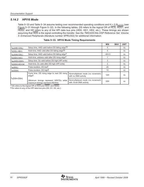
Documentation Support5.14.2 HPI16 ModeTable 5−33 and Table 5−34 assume testing over recommended operating conditions and H = 0.5t c(CO) (seeFigure 5−31 through Figure 5−32). In the following tables, DS refers to the logical OR of HCS, HDS1, andHDS2, and HD refers to any of the HPI data bus pins (HD0, HD1, HD2, etc.). These timings are shownassuming that HDS is the signal controlling the transfer. See the TMS320C54x DSP Reference Set, Volume5: Enhanced Peripherals (literature number SPRU302) for additional information.Table 5−33. HPI16 Mode Timing RequirementsMIN MAX UNITtsu(HBV-DSL) Setup time, HAD valid before DS falling edge†‡ 5 nsth(DSL-HBV) Hold time, HAD valid after DS falling edge†‡ 5 nstsu(HAV-DSL) Setup time, HAD valid before DS falling edge† −4H+3 nsth(DSH-HAV) Hold time, address valid after DS rising edge† 1 nstsu(HDV-DSH) Setup time, Dx valid before DS high (HPI write) 3 nsth(DSH-HDV)W Hold time, Dx valid after DS high (HPI write) 2 nstw(DSL) Pulse duration, DS low‡ 20 nstw(DSH) Pulse duration, DS high‡ 10 nsCycle time, DS rising edge to next DS risingedge‡tc(DSH-DSH)(Minimum timings represent WRITEs whilemaximum timings represent READs)† DS refers to the logical OR of HCS and HDS1 and HDS2.‡ Dx refers to any of the HPI data bus pins (D0, D1, D2, etc.).Nonmultiplexed mode (no increment)with no DMA activity.Nonmultiplexed mode (no increment)with 16-bit DMA activity.12H20Hnsns82 SPRS082FApril 1999 − Revised October 2008