TMS320VC5409 Fixed-Point Digital Signal ... - Texas Instruments
TMS320VC5409 Fixed-Point Digital Signal ... - Texas Instruments
TMS320VC5409 Fixed-Point Digital Signal ... - Texas Instruments
- No tags were found...

You also want an ePaper? Increase the reach of your titles
YUMPU automatically turns print PDFs into web optimized ePapers that Google loves.
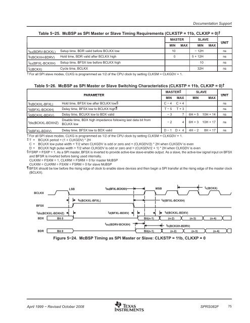
Documentation SupportTable 5−25. McBSP as SPI Master or Slave Timing Requirements (CLKSTP = 11b, CLKXP = 0) †MASTER SLAVEMIN MAX MIN MAXUNITtsu(BDRV-BCKXL) Setup time, BDR valid before BCLKX low 10 − 12H nsth(BCKXH-BDRV) Hold time, BDR valid after BCLKX high 0 5 + 12H nstsu(BFXL-BCKXH) Setup time, BFSX low before BCLKX high 10 nstc(BCKX) Cycle time, BCLKX 32H ns† For all SPI slave modes, CLKG is programmed as 1/2 of the CPU clock by setting CLKSM = CLKGDV = 1.Table 5−26. McBSP as SPI Master or Slave Switching Characteristics (CLKSTP = 11b, CLKXP = 0) †PARAMETERMASTER‡SLAVEMIN MAX MIN MAXth(BCKXL-BFXL) Hold time, BFSX low after BCLKX low§ C − 4 C + 4 nstd(BFXL-BCKXH) Delay time, BFSX low to BCLKX high T − 5 T + 3 nstd(BCKXL-BDXV) Delay time, BCLKX low to BDX valid − 3 7 6H + 5 10H + 14 nstdis(BCKXL-BDXHZ)Disable time, BDX high impedance following last data bit fromBCLKX lowUNIT− 2 4 6H + 3 10H + 17 nstd(BFXL-BDXV) Delay time, BFSX low to BDX valid D − 1 D + 4 4H − 2 8H + 17 ns† For all SPI slave modes, CLKG is programmed as 1/2 of the CPU clock by setting CLKSM = CLKGDV = 1.‡ T = BCLKX period = (1 + CLKGDV) * 2HC = BCLKX low pulse width = T/2 when CLKGDV is odd or zero and = (CLKGDV/2) * 2H when CLKGDV is evenD = BCLKX high pulse width = T/2 when CLKGDV is odd or zero and = (CLKGDV/2 + 1) * 2H when CLKGDV is even§ FSRP = FSXP = 1. As a SPI master, BFSX is inverted to provide active-low slave-enable output. As a slave, the active-low signal input on BFSXand BFSR is inverted before being used internally.CLKXM = FSXM = 1, CLKRM = FSRM = 0 for master McBSPCLKXM = CLKRM = FSXM = FSRM = 0 for slave McBSP BFSX should be low before the rising edge of clock to enable slave devices and then begin a SPI transfer at the rising edge of the master clock(BCLKX).BCLKXLSBt su(BFXL-BCKXH)MSBt c(BCKX)t h(BCKXL-BFXL)t d(BFXL-BCKXH)BFSXt dis(BCKXL-BDXHZ)t d(BFXL-BDXV)t d(BCKXL-BDXV)BDXBDRBit 0 Bit(n-1) (n-2) (n-3) (n-4)t su(BDRV-BCKXH)t h(BCKXH-BDRV)Bit 0 Bit(n-1) (n-2) (n-3) (n-4)Figure 5−24. McBSP Timing as SPI Master or Slave: CLKSTP = 11b, CLKXP = 0April 1999 − Revised October 2008SPRS082F75