research activities in 2007 - CSEM
research activities in 2007 - CSEM
research activities in 2007 - CSEM

You also want an ePaper? Increase the reach of your titles
YUMPU automatically turns print PDFs into web optimized ePapers that Google loves.
Flip Chip Bond<strong>in</strong>g on Polymers – Die Attach and Leak-Tight Seal<strong>in</strong>g<br />
M. Fretz, T. Harvey • , J. Auerswald, N. Schmid, A-C. Pliska, C. Bosshard<br />
A bond<strong>in</strong>g process for sens<strong>in</strong>g elements on PMMA based platforms or vice versa was developed. A r<strong>in</strong>g of anisotropic conductive adhesive (ACA)<br />
forms a cavity between PMMA die and silicon platform. Seal<strong>in</strong>g tests were carried out. This process is suited for dies too small for a micro-gasket<br />
approach.<br />
As a low cost thermoplastic material, PMMA is specially suited<br />
for microfluidic applications and not only for disposable<br />
devices. Often a sample to be <strong>in</strong>spected must be guided to<br />
the appropriate sensor element through a fluidic channel or<br />
network. Hence, flip chip bond<strong>in</strong>g of the active element on a<br />
PMMA platform is a suitable <strong>in</strong>tegration approach. Two tasks<br />
arise: Flip chip bond<strong>in</strong>g must provide electrical contact, and<br />
the sens<strong>in</strong>g area of the chip must be hermetically closed<br />
aga<strong>in</strong>st the ambient air. Both can be achieved by the use of<br />
anisotropic conductive adhesive (ACA). In this report, the<br />
bond<strong>in</strong>g process of a PMMA die mounted on a silicon platform<br />
with a r<strong>in</strong>g of ACA is described. Electrical connection between<br />
PMMA and silicon was demonstrated before <strong>in</strong> [1] .<br />
2<br />
1<br />
3<br />
ACA r<strong>in</strong>g<br />
Cavity<br />
4<br />
Figure 1: Die attachment process: The gold studs are placed on the<br />
pads of a PMMA die (1) and flattened (2). Then the flipped die is<br />
mounted on the silicon platform (3), on which a r<strong>in</strong>g of anisotropic<br />
conductive adhesive was dispensed. F<strong>in</strong>ally, the cavity is connected<br />
to the seal<strong>in</strong>g test set up (4).<br />
First, two holes were drilled through the ~5 x 5 x 2 mm 3<br />
PMMA dies. Then, a standard wire bonder was used to place<br />
gold studs on the PMMA (see Figure 1). After gold stud<br />
bump<strong>in</strong>g, a r<strong>in</strong>g of ACA was dispensed on the silicon platform,<br />
followed by the attachment of the flipped PMMA die on the<br />
silicon (Figure 2). The attachment step is critical, because<br />
ACA requires heat (m<strong>in</strong>imum 125 °C) and pressure. But<br />
PMMA will warp under load when exposed to temperatures<br />
above ~100 °C (for more details, see [1] ). Tests were carried<br />
out to evaluate the seal<strong>in</strong>g quality of the ACA: Air was<br />
pumped through the cavity which was connected to a dead<br />
end pressure sensor (for more details, see [2] ).The pressure<br />
was <strong>in</strong>creased until it exceeded 1 bar. Then the leakage of the<br />
cavity was measured for ten m<strong>in</strong>utes, as well as the leakage<br />
of the tub<strong>in</strong>g system alone. The result is plotted <strong>in</strong> Figure 3.<br />
No breakdown of the pressure was observed with<strong>in</strong> twenty<br />
m<strong>in</strong>utes. The decrease <strong>in</strong> pressure is due to the tub<strong>in</strong>g and<br />
connectors, as Figure 3 shows. Seal<strong>in</strong>g with ACA can,<br />
therefore, be a suitable approach for microfluidic applications<br />
which require flip chip bond<strong>in</strong>g of small dies.<br />
Metal pads<br />
ACA r<strong>in</strong>g<br />
Drilled holes<br />
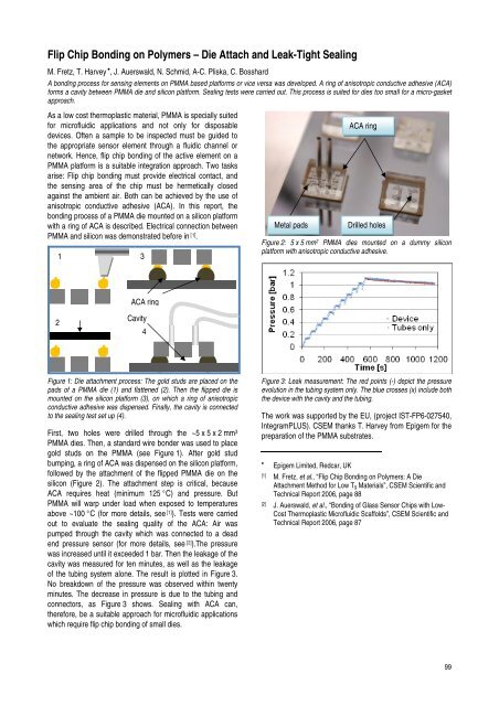
Figure 2: 5 x 5 mm 2 PMMA dies mounted on a dummy silicon<br />
platform with anisotropic conductive adhesive.<br />
Figure 3: Leak measurement: The red po<strong>in</strong>ts (-) depict the pressure<br />
evolution <strong>in</strong> the tub<strong>in</strong>g system only. The blue crosses (x) <strong>in</strong>clude both<br />
the device with the cavity and the tub<strong>in</strong>g.<br />
The work was supported by the EU, (project IST-FP6-027540,<br />
IntegramPLUS). <strong>CSEM</strong> thanks T. Harvey from Epigem for the<br />
preparation of the PMMA substrates.<br />
•<br />
Epigem Limited, Redcar, UK<br />
[1] M. Fretz, et al., “Flip Chip Bond<strong>in</strong>g on Polymers: A Die<br />
Attachment Method for Low Tg Materials”, <strong>CSEM</strong> Scientific and<br />
Technical Report 2006, page 88<br />
[2] J. Auerswald, et al., “Bond<strong>in</strong>g of Glass Sensor Chips with Low-<br />
Cost Thermoplastic Microfluidic Scaffolds”, <strong>CSEM</strong> Scientific and<br />
Technical Report 2006, page 87<br />
99