research activities in 2007 - CSEM
research activities in 2007 - CSEM
research activities in 2007 - CSEM

Create successful ePaper yourself
Turn your PDF publications into a flip-book with our unique Google optimized e-Paper software.
Optoelectronic Test Equipment for Image Sensors and Systems Qualification<br />
A. Baumgartner<br />
The test<strong>in</strong>g of a circuit is an essential but quite expensive step <strong>in</strong> the production flow of semiconductor devices. Frequently <strong>CSEM</strong> customers are<br />
look<strong>in</strong>g for small volume production with a high quality level. Therefore a test<strong>in</strong>g environment has been set up to support production verification and<br />
qualification <strong>in</strong>-house with moderate <strong>in</strong>vestments and <strong>in</strong> a very short time after prototype evaluation. This is achieved thanks to the development of<br />
very similar rout<strong>in</strong>es for both evaluation measurements at the prototype level and for production verification.<br />
Follow<strong>in</strong>g the evaluation of the first prototypes, the set-up of a<br />
fully automatic test system for production test<strong>in</strong>g typically<br />
requires a large effort and high <strong>in</strong>vestments.<br />
Quite often for products result<strong>in</strong>g from “lead<strong>in</strong>g edge” <strong>research</strong><br />
projects, the standard <strong>in</strong>dustry levels of quality are expected<br />
but for significantly lower quantities. Furthermore the<br />
development of test plans for automatic test equipments<br />
(ATE) can be quite costly due to the high time pressure for<br />
rapid development cycles and a quick ramp up of the<br />
production.<br />
Prototype evaluation is a key phase <strong>in</strong> the development of<br />
novel image sensors. This evaluation can be very timeconsum<strong>in</strong>g<br />
and needs to be repeated for each new sensor<br />
circuit. The measurements done dur<strong>in</strong>g evaluation are similar<br />
to the test<strong>in</strong>g cycles for the production verification. For largevolume<br />
production, test<strong>in</strong>g is normally done on dedicated test<br />
systems. In this project, a cost-effective evaluation system for<br />
production test<strong>in</strong>g was <strong>in</strong>vestigated and implemented for low<br />
volume production.<br />
To be able to verify a device <strong>in</strong> a short time, special test<strong>in</strong>g<br />
features and design for test (DfT) generally have to be<br />
implemented:<br />
• Insertion of structural test<strong>in</strong>g for digital design (blocks)<br />
such as the exchange of flip-flops with scan flip-flops<br />
• Insertion of special dedicated “test“ registers to guarantee<br />
the control- and observability of analogue blocks<br />
This work has to be done dur<strong>in</strong>g the design phase and the<br />
fault coverage of these tests has to be checked before the end<br />
of the design phase. Therefore, a test concept for production<br />
test<strong>in</strong>g needs to be done and elaborated before the project<br />
design phase starts.<br />
For manufactured optical semiconductors, the follow<strong>in</strong>g<br />
procedure is used:<br />
• Manufacture wafers with PCM structures (=dedicated test<br />
structures), verify PCM structures <strong>in</strong> wafer fabrication site<br />
• Samples are first tested us<strong>in</strong>g a (wafer) prober and a<br />
needlecard (probecard) to contact the pads. The fail<strong>in</strong>g<br />
samples are marked. This first measurement is done <strong>in</strong> a<br />
clean atmosphere (open wafers) <strong>in</strong> the pre-test site, e.g. <strong>in</strong><br />
a clean room at <strong>CSEM</strong> <strong>in</strong> Zurich. To guarantee correct<br />
operation over the full temperature range, this first test is<br />
done at one temperature with<strong>in</strong> the specified limits (e.g.<br />
hot)<br />
• The good samples are packaged <strong>in</strong> s<strong>in</strong>gle-die<br />
packages,on multi-die “chip-carriers” like Multi-Chip-<br />
Packages/Multi-Chip-Modules (MCP/MCM) or bonded<br />
directly on circuit boards (e.g. on “flexpr<strong>in</strong>ts”)<br />
• The packaged samples are tested a second time at a<br />
different temperature.<br />
An automatic test system for evaluation and small-volume<br />
production test<strong>in</strong>g us<strong>in</strong>g a National Instruments LabVIEW® -<br />
based system was chosen as a solution for <strong>CSEM</strong>. For cost<br />
reasons the measurement hardware is based on PC<br />
components. It consists of a PC with 19 PXI cards (<strong>in</strong> 2<br />
external racks), a semiautomatic prober <strong>in</strong> a dark cab<strong>in</strong>et and<br />
an Ulbricht sphere.<br />
With the above described hardware the ma<strong>in</strong> challenge is the<br />
capability to test semiconductors very fast. Therefore,<br />
additional external equipment consist<strong>in</strong>g of a logic analyzer<br />
and a pattern generator were <strong>in</strong>tegrated <strong>in</strong>to the system. The<br />
complete test<strong>in</strong>g set-up is controlled from LabVIEW with the<br />
TestStand add-on LabVIEW tool.<br />
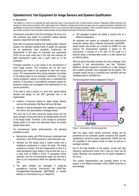
The test equipment looks as displayed <strong>in</strong> Figure 1.<br />
PXI l<strong>in</strong>k<br />
Logic<br />
Analyzer<br />
PXI<br />
System<br />
Ulbricht<br />
sphere<br />
RS232<br />
GPIB<br />
PC1: LabVIEW 8.5<br />
XP<br />
DUT<br />
Prober<br />
RS232<br />
PC2: Proberbech<br />
NT4.0<br />
Figure 1: Schematics of the test equipement.<br />
Dark Room<br />
Clean Room<br />
With this setup, small volume production test<strong>in</strong>g can be<br />
performed and an automatic system evaluation flow (system<br />
qualification) can/will be easily implemented. <strong>CSEM</strong> has now<br />
the possibility to test optical circuits on wafer as well as on<br />
packaged samples.<br />
Due to the high flexibility of this system, circuits with high<br />
frequency requirements and/or with a high p<strong>in</strong> count can be<br />
tested. Moreover new equipment can be easily <strong>in</strong>tegrated <strong>in</strong><br />
the future.<br />
This system implementation was possible thanks to the<br />
support of the Wilsdorf foundation which <strong>CSEM</strong> would like to<br />
acknowledge.<br />
35