research activities in 2007 - CSEM
research activities in 2007 - CSEM
research activities in 2007 - CSEM

Create successful ePaper yourself
Turn your PDF publications into a flip-book with our unique Google optimized e-Paper software.
MicroMec – Microtechnology for Silicon Compliant Structures<br />
C. Verjus, J.-M. Major, T. Overstolz, A. Hoogerwerf, A. Ibzazene, A. Neels, A. Schifferle, A. Dommann<br />
The target of this project is the development of a microfabricated silicon compliant structure for mechanical applications and its understand<strong>in</strong>g of the<br />
ag<strong>in</strong>g behaviour.<br />
MEMS can be made highly reliable, but it must however be<br />
noted that the failure modes of MEMS can be different from<br />
those of solid-state electronics. Therefore test<strong>in</strong>g techniques<br />
must be developed to accelerate MEMS-specific failures [1] .<br />
Monocrystall<strong>in</strong>e material and, especially, silicon is<br />
preferentially used due to its potential resistance aga<strong>in</strong>st<br />
ag<strong>in</strong>g. However, quantified results of this fact are rarely<br />
published. The reasons are manifold; however they are also<br />
related to the surface roughness as well as to the defect<br />
concentration of the etched surfaces due to the ion<br />
bombardment [2] .<br />
Deep reactive ion etch<strong>in</strong>g (DRIE) of silicon-on-<strong>in</strong>sulator (SOI)<br />
substrates allows the fabrication of structures with arbitrary<br />
shapes (2D) that are vertically extruded by remov<strong>in</strong>g excess<br />
silicon.<br />
Test structures can be built from s<strong>in</strong>gle crystall<strong>in</strong>e silicon by<br />
DRIE processes. Mechanical tests on these structures <strong>in</strong><br />
relation with simulations of stresses and the experimental<br />
determ<strong>in</strong>ation of the stra<strong>in</strong> / stress behavior and defect<br />
analysis by High Resolution Diffraction Methods (HRXRD)<br />
give very important <strong>in</strong>formation about the device and its long<br />
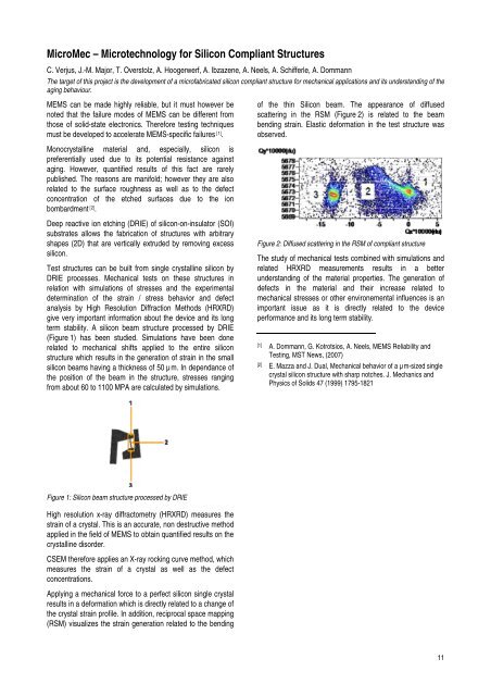
term stability. A silicon beam structure processed by DRIE<br />
(Figure 1) has been studied. Simulations have been done<br />
related to mechanical shifts applied to the entire silicon<br />
structure which results <strong>in</strong> the generation of stra<strong>in</strong> <strong>in</strong> the small<br />
silicon beams hav<strong>in</strong>g a thickness of 50 µm. In dependance of<br />
the position of the beam <strong>in</strong> the structure, stresses rang<strong>in</strong>g<br />
from about 60 to 1100 MPA are calculated by simulations.<br />
Figure 1: Silicon beam structure processed by DRIE<br />
High resolution x-ray diffractometry (HRXRD) measures the<br />
stra<strong>in</strong> of a crystal. This is an accurate, non destructive method<br />
applied <strong>in</strong> the field of MEMS to obta<strong>in</strong> quantified results on the<br />
crystall<strong>in</strong>e disorder.<br />
<strong>CSEM</strong> therefore applies an X-ray rock<strong>in</strong>g curve method, which<br />
measures the stra<strong>in</strong> of a crystal as well as the defect<br />
concentrations.<br />
Apply<strong>in</strong>g a mechanical force to a perfect silicon s<strong>in</strong>gle crystal<br />
results <strong>in</strong> a deformation which is directly related to a change of<br />
the crystal stra<strong>in</strong> profile. In addition, reciprocal space mapp<strong>in</strong>g<br />
(RSM) visualizes the stra<strong>in</strong> generation related to the bend<strong>in</strong>g<br />
of the th<strong>in</strong> Silicon beam. The appearance of diffused<br />
scatter<strong>in</strong>g <strong>in</strong> the RSM (Figure 2) is related to the beam<br />
bend<strong>in</strong>g stra<strong>in</strong>. Elastic deformation <strong>in</strong> the test structure was<br />
observed.<br />
Figure 2: Diffused scatter<strong>in</strong>g <strong>in</strong> the RSM of compliant structure<br />
The study of mechanical tests comb<strong>in</strong>ed with simulations and<br />
related HRXRD measurements results <strong>in</strong> a better<br />
understand<strong>in</strong>g of the material properties. The generation of<br />
defects <strong>in</strong> the material and their <strong>in</strong>crease related to<br />
mechanical stresses or other environemental <strong>in</strong>fluences is an<br />
important issue as it is directly related to the device<br />
performance and its long term stability.<br />
[1] A. Dommann, G. Kotrotsios, A. Neels, MEMS Reliability and<br />
Test<strong>in</strong>g, MST News, (<strong>2007</strong>)<br />
[2] E. Mazza and J. Dual, Mechanical behavior of a µm-sized s<strong>in</strong>gle<br />
crystal silicon structure with sharp notches. J. Mechanics and<br />
Physics of Solids 47 (1999) 1795-1821<br />
11