research activities in 2007 - CSEM
research activities in 2007 - CSEM
research activities in 2007 - CSEM

You also want an ePaper? Increase the reach of your titles
YUMPU automatically turns print PDFs into web optimized ePapers that Google loves.
Towards Plasmon Enhanced Detectors<br />
L. A. Dunbar, M. Guillaumée, R. Eckert, E. Franzi, R. P. Stanley<br />
Surface plasmons play a key role <strong>in</strong> the recent experiments on extra-ord<strong>in</strong>ary optical transmission through nano-structured metals. By tailor<strong>in</strong>g<br />
these nanostructures they can be used to enhance optical transmission, with polarisation and spectral selection. Incorporat<strong>in</strong>g these nanostructures<br />
directly onto photon detectors can improve their performance.<br />
To enhance the signal to noise ratio of detectors one can<br />
either enhance the signal or reduce the noise. Recently<br />
Ebbesen et al [1] measured extraord<strong>in</strong>ary optical transmission<br />
through sub-wavelength holes <strong>in</strong> an otherwise opaque metal.<br />
By exploit<strong>in</strong>g this effect, light can be harvested on<br />
photodetectors and the signal to noise ratio can be <strong>in</strong>creased.<br />
Currently <strong>CSEM</strong> is fabricat<strong>in</strong>g metallic nanostructures on<br />
image sensors to do just this. Additionally these<br />
nanostructured metallic films can act as spectral and<br />
polarization filters or a comb<strong>in</strong>ation of the two.<br />
Initial trials have been made to <strong>in</strong>vestigate the enhanced<br />
transmission through a s<strong>in</strong>gle slit surrounded by a series of<br />
grooves. Incident light is converted <strong>in</strong>to a surface wave<br />
(plasmon) by the periodic array of grooves. The light is<br />
transported along the surface towards the central slit. This<br />
allows light which does not fall on the central slit, to pass<br />
through the slit and <strong>in</strong>crease the signal that can be detected<br />
with the detector under the slit. As the shot noise depends on<br />
the size detector, <strong>in</strong>creas<strong>in</strong>g the signal whilst ma<strong>in</strong>ta<strong>in</strong><strong>in</strong>g the<br />
same detector size <strong>in</strong>creases the signal to noise ratio. Initial<br />
results give a factor of 5 enhancement per surface area over a<br />
spectral bandwidth of 25 nm.<br />
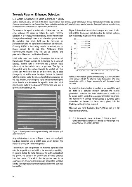
Figure 1: Scann<strong>in</strong>g electron micrograph show<strong>in</strong>g a slit delimited by 5<br />
groove structures<br />
A typical structure is shown <strong>in</strong> Figure 1. Here 140 nm of gold<br />
has been deposited onto a <strong>CSEM</strong> made Vision Sensor. The<br />
metal has a very low surface roughness.<br />
The structures can be optimised for improved signal to noise<br />
ratio, for a specific spectral width or for polarisation sensitivity.<br />
In order to do this the metal thickness, the width and depth of<br />
the groove, the period of the grooves and the <strong>in</strong>itial distance<br />
from the centre of the slit to the first groove need to be<br />
optimised. Slit structures are <strong>in</strong>tr<strong>in</strong>sically polarisation selective<br />
and by vary<strong>in</strong>g these parameters spectral selectivity can also<br />
be modified.<br />
50<br />
Figure 2 shows the transmission through a structured film for<br />
different film thicknesses and shows that the spectral features<br />
can be tuned by vary<strong>in</strong>g the metal thickness.<br />
Figure 2: Transmission spectra calculated us<strong>in</strong>g 2D-F<strong>in</strong>ite Difference<br />
Time Doma<strong>in</strong> (FDTD) for different metal thicknesses. The peak<br />
transmission shifts to longer wavelengths with <strong>in</strong>creased metal<br />
thickness.<br />
To obta<strong>in</strong> the desired optical properties is not straight forward<br />
as there is a complex <strong>in</strong>terplay between the various<br />
parameters. Moreover the metal smoothness is crucial both<br />
for losses and to obta<strong>in</strong> the necessary fabrication tolerances.<br />
The fabrication of tailored nanostructures is currently be<strong>in</strong>g<br />
undertaken by focused ion beam which gives both the<br />
flexibility and the precision required.<br />
This work was partly funded by the PLEAS as part of a EU<br />
Project <strong>in</strong> framework 6.<br />
[1] T. W. Ebbesen, H. J. Lezec, H. Ghaemi, T. Thio, P. A. Wolf,<br />
"Extraord<strong>in</strong>ary optical transmission through sub-wavelength hole<br />
arrays," Nature 391, (1998), 667-669