research activities in 2007 - CSEM
research activities in 2007 - CSEM
research activities in 2007 - CSEM

Create successful ePaper yourself
Turn your PDF publications into a flip-book with our unique Google optimized e-Paper software.
Towards an Optical Switch with J-aggregates Monolayers<br />
R. Eckert, J. D<strong>in</strong>t<strong>in</strong>ger • , T. Ebbesen • , R. P. Stanley<br />
J-aggregates are an efficient non-l<strong>in</strong>ear optical material. They have been successfully used <strong>in</strong> ultrafast all optical switches, which exploit plasmonic<br />
effects of nano-structured metal surfaces. This work aims to replace 100 nm thick J-aggregate layers <strong>in</strong> such switches by a monolayer of<br />
J-aggregates us<strong>in</strong>g a unique deposition technique.<br />
Extraord<strong>in</strong>ary optical transmission (EOT) through an array of<br />
subwavelength holes drilled <strong>in</strong> a metal film relies on the<br />
<strong>in</strong>terplay of surface plasmons (SP) with the periodicity of the<br />
nanostructure to make the otherwise opaque film transparent.<br />
EOT is not only a very active field of basic <strong>research</strong> but is<br />
currently f<strong>in</strong>d<strong>in</strong>g its way <strong>in</strong>to real world applications and<br />
devices.<br />
The concept of an ultrafast all–optical switch, which exploits<br />
EOT, has been demonstrated recently [1] . Its basic component<br />
is a gold film with an array of holes covered with J-aggregates<br />
(Figure 1). J-aggregates (JA) are formed from cyan<strong>in</strong>e<br />
molecules and have well-def<strong>in</strong>ed absorption bands. The<br />
difference between their ground and excited states is sufficient<br />
to change the transmission properties of the array.<br />
Consequently, one beam of light (the probe beam) can be<br />
switched on and off by excit<strong>in</strong>g the JA with a second beam of<br />
light (pump beam).<br />
Figure 1: Concept of an all optical switch based on EOT<br />
In the orig<strong>in</strong>al work the JA were randomly dispersed <strong>in</strong> a<br />
200 nm thick polymer film coated on one side of the hole<br />
array. The present work aims at achiev<strong>in</strong>g the same effect by<br />
us<strong>in</strong>g only a monolayer of highly ordered JA formed by a<br />
process developed at <strong>CSEM</strong> us<strong>in</strong>g a template of selfassembled<br />
dendrimers. Both, the remarkable absorption<br />
efficiency of these monolayers and the possibility of coat<strong>in</strong>g<br />
both sides of the hole array <strong>in</strong>stead of only one offer the<br />
potential to achieve bigger switch<strong>in</strong>g amplitudes between on<br />
and off states of the device.<br />
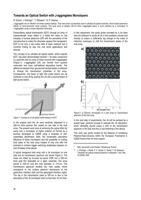
A typical hexagonal hole array with a JA monolayer on one<br />
side and its transmission spectrum are shown Figure 2. The<br />
holes are milled by focused ion beam (FIB) <strong>in</strong>to a 200 nm<br />
thick gold film deposited on a glass substrate. The array<br />
period is 525 nm and the hole diameter is 175 nm. The<br />
transmission spectrum exhibits two ma<strong>in</strong> peaks, which<br />
correspond to the surface plasmon resonances at the<br />
gold/JA/air <strong>in</strong>terface (left) and the glass/gold <strong>in</strong>terface (right).<br />
The dip <strong>in</strong> the transmission peak at 550 nm is due to the<br />
absorption of the JA monolayer which is less than 10 nm thick.<br />
48<br />
In this experiment, the pump power provided by a cw laser<br />
was not sufficient to excite all JA <strong>in</strong> the excitation volume and<br />
thereby to <strong>in</strong>duce a sufficiently big change of the <strong>in</strong>dex of<br />
refraction necessary to shift the transmission peaks of the<br />
hole array.<br />
Figure 2: a) Electron micrograph of a hole array b) Transmission<br />
spectrum of the hole array<br />
In the next step of experiments, the JA will be pumped by a<br />
pulsed laser, powerful enough to saturate the JA absorption,<br />
which ultimately should cause a shift of the transmission<br />
spectrum to the blue and thus a real switch<strong>in</strong>g of the device.<br />
This work was partly funded by the Network of excellence<br />
Plasmon-Nano-Devices with<strong>in</strong> the European Framework 6.<br />
<strong>CSEM</strong> thanks them for their support.<br />
•<br />
ISIS, Université Louis Pasteur, Strasbourg, France<br />
[1] J. D<strong>in</strong>t<strong>in</strong>ger, I. Robel, P. V. Kamat, C. Genet, T. W. Ebbesen,<br />
“Terahertz all-optical molecule-plasmon modulation”, Adv. Mat.<br />
18 (2006) 1645