research activities in 2007 - CSEM
research activities in 2007 - CSEM
research activities in 2007 - CSEM

Create successful ePaper yourself
Turn your PDF publications into a flip-book with our unique Google optimized e-Paper software.
Direct Modulation RF Transmitter and Super-Heterodyne Low-IF Receiver Development<br />
Platform for 868 MHz and 915 MHz ISM Bands<br />
M. Contaldo, E. Le Roux, D. Ruffieux, P. Volet, M. Kucera, N. Raemy, F. Giroud, F. Pengg, S. Gyger, C. Arm, P. Heim, F. Kaess,<br />
V. Peiris<br />
This paper presents the design of a radio development platform suited for develop<strong>in</strong>g ultra low-power high-performance narrow-band RF<br />
transceivers. In particular, this platform will be used for validat<strong>in</strong>g an 868 MHz/915 MHz RF IC featur<strong>in</strong>g up to ±200kHz modulation bandwidth for<br />
different constant-envelope modulation schemes, and consum<strong>in</strong>g below 3 mA current <strong>in</strong> receive mode under a very-low 1 V supply.<br />
For wireless sensor networks or body-area networks for biomedical<br />
and lifestyle applications, the need of a m<strong>in</strong>iature and<br />
ultra-low power radio transceiver is mandatory to achieve<br />
multi-year autonomy with un-obtrusive embodiment.<br />
Ultra low-power consumption (below 3 mA under 1 V supply <strong>in</strong><br />
receive mode) has been demonstrated for radios operat<strong>in</strong>g <strong>in</strong><br />
sub-GHz bands and us<strong>in</strong>g simple FSK/OOK modulation<br />
schemes [1] . On the other hand, the requirements <strong>in</strong> terms of<br />
modulation schemes and bandwidths happen to differ<br />
significantly depend<strong>in</strong>g on the targeted applications. The<br />
design of an optimal radio architecture rema<strong>in</strong>s thus a<br />
complex task as the impact and the added value of various<br />
modulation strategies must be quantified carefully before f<strong>in</strong>al<br />
<strong>in</strong>tegration, <strong>in</strong> particular for low-power radios.<br />
Although high- and low-level simulations help for prelim<strong>in</strong>ary<br />
validation, a given radio architecture may be fully validated<br />
only with real-world measurements <strong>in</strong>clud<strong>in</strong>g complex channel<br />
and <strong>in</strong>terference situations which are difficult to simulate. To<br />
address this issue, this paper presents an <strong>in</strong>termediate<br />
approach, <strong>in</strong> the form of a microelectronics-oriented hardware<br />
development platform, as depicted <strong>in</strong> Figure 1.<br />
Figure 1: Development platform block diagram<br />
This approach with a programmable FPGA-based back-end<br />
enables the development and validation of various modulation<br />
schemes with a high degree of flexibility, by programm<strong>in</strong>g<br />
baseband process<strong>in</strong>g algorithms <strong>in</strong>to the FPGA, and<br />
characteriz<strong>in</strong>g the l<strong>in</strong>k performance before full <strong>in</strong>tegration.<br />
Because the front-end is a low-power RF IC, the architecture<br />
of the platform is very close to that of an <strong>in</strong>tegrated circuit.<br />
Hence the design of a complete transceiver comb<strong>in</strong><strong>in</strong>g both<br />
sections on a s<strong>in</strong>gle die will be enabled with a low risk level.<br />
The RF front-end IC <strong>in</strong>cludes the transmitter (Tx), receiver<br />
(Rx) and frequency synthesizer (PLL) circuitry, from the<br />
antenna <strong>in</strong>put towards the analog baseband, without rely<strong>in</strong>g<br />
on any other external active components. The Rx/Tx is<br />
designed for operation <strong>in</strong> the 868/915 MHz bands. The FPGA<br />
embeds the digital parts such as the modulation/demodulation<br />
section of the radio, the control for the RF front-end IC and the<br />
<strong>in</strong>terfaces. For the slow digital configuration signals, e.g.<br />
analog sub-block bias sett<strong>in</strong>gs, the configuration is done<br />
through serial l<strong>in</strong>k (I2C). For fast digital signal, i.e. the RF<br />
synthesizer sett<strong>in</strong>gs, the configuration is done through a<br />
parallel bus. The FPGA clock signal is generated on the RF<br />
front-end IC, therefore their association does not need any<br />
additional circuit.<br />
With<strong>in</strong> the RF front-end IC, the transmitter is based on a direct<br />
modulation architecture. The frequency synthesizer is<br />
implemented by means of a fractional-N PLL employ<strong>in</strong>g a<br />
3rd order MASH sigma delta modulator, tak<strong>in</strong>g advantage of its<br />
beneficial noise shap<strong>in</strong>g effect. The external loop filter and the<br />
programmable charge pump permit a good customizability of<br />
the synthesizer performances. The synthesized signal is then<br />
directly coupled to the power amplifier and directed to a SAW<br />
filter, before reach<strong>in</strong>g the antenna. The receiver is based on a<br />
heterodyne low-IF architecture that down-converts the RF<br />
signal <strong>in</strong>to at 96-103 MHz <strong>in</strong>termediate frequency and then to<br />
75-150 kHz, where it can be filtered. The signal is then<br />
converted <strong>in</strong> the digital doma<strong>in</strong> us<strong>in</strong>g an <strong>in</strong>tegrated<br />
phase-ADC whose output drives the FPGA to allow the design<br />
and measurement of different demodulations [2]<br />
The ma<strong>in</strong> specifications of the radio are up to ±200 kHz<br />
modulation bandwidth, with a 3 mA current consumption <strong>in</strong> Rx<br />
for -105 dBm sensitivity, and 40 mA <strong>in</strong> Tx for a 10 dBm output<br />
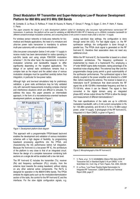
power, under 1V supply. A photograph of the RF front-end IC,<br />
<strong>in</strong>tegrated <strong>in</strong> 0.18um CMOS, is given <strong>in</strong> Figure 2.<br />
Figure 2: Microphotograph of the RF front-end IC<br />
[1] V. Peiris, et al., “A 1V 433/868MHz 25kb/s-FSK 2kb/s-OOK RF<br />
Transceiver SoC <strong>in</strong> Standard Digital 0.18 μm CMOS,” <strong>in</strong> Int.<br />
Solid-State Circ. Conf. Dig. of Tech. Papers, Feb. 2005, 258-259<br />
[2] E. Le Roux, “Low Power Flexible Digital Demodulator for<br />
Integrated RF Transceiver”, <strong>CSEM</strong> Scientific and Technical<br />
Report 2006, page 27<br />
27