research activities in 2007 - CSEM
research activities in 2007 - CSEM
research activities in 2007 - CSEM

Create successful ePaper yourself
Turn your PDF publications into a flip-book with our unique Google optimized e-Paper software.
UWB Antenna with Improved Bandwidth and Spatial Diversity us<strong>in</strong>g RF-MEMS Switches<br />
Q. Xu, L. Petit, J. R. Farserotu<br />
An UWB dual patch antenna with optimized bandwidth from 5.5 to 9.7 GHz was developed. Together with a RF MEMS based switch comb<strong>in</strong><strong>in</strong>g<br />
circuit, the UWB antenna allows construction of a reconfigurable unit that provides multiple-direction radiation.<br />
With<strong>in</strong> the project e-SENSE, <strong>CSEM</strong> has undertaken R&D on<br />
energy efficient FR solutions for Wireless Sensor Network<br />
(WSN). To successfully address the different scenarios and<br />
enhance the overall system performance, a very promis<strong>in</strong>g<br />
option is to add more functionality to the antenna subsystem,<br />
and focus on pattern reconfigurability of the UWB antennas.<br />
The motivations to address radiation pattern reconfigurability<br />
are the follow<strong>in</strong>g:<br />
• Range extension<br />
• Direction Of Arrival (DOA) estimation<br />
• Enhanced coexistence (Multiple users, multipath rejection)<br />
UWB antenna design – a structure of stacked and notched<br />
dual-patch has been adopted to achieve the bandwidth<br />
enhancement. Parameters, <strong>in</strong>clud<strong>in</strong>g the size of the patches,<br />
the slot length, the microstrip feed position, the spacer<br />
thickness, as well as the dimensions of the notches, that<br />
impact the bandwidth performance have been optimized<br />
simultaneously <strong>in</strong> simulations. The enhanced impedance<br />
match<strong>in</strong>g bandwidth rang<strong>in</strong>g from 5.5 GHz to 9.7 GHz has<br />
been achieved and has shown good agreement with<br />
measured results (Figure 1).<br />
80<br />
S11 Mag [dB]<br />
0<br />
-5<br />
-10<br />
-15<br />
-20<br />
-25<br />
-30<br />
Measurement<br />
Theoretical computation<br />
-35<br />
4 5 6 7 8 9 10 11 12<br />
Frequency [GHz]<br />
Figure 1: Measured and simulated impedance bandwidth<br />
RF-MEMS comb<strong>in</strong><strong>in</strong>g circuit – a switch comb<strong>in</strong><strong>in</strong>g circuit has<br />
been developed and is presented <strong>in</strong> Figure 2. RF MEMS for<br />
reconfigurable antennas and beam form<strong>in</strong>g networks (BFN)<br />
exhibit outstand<strong>in</strong>g performances <strong>in</strong> terms of l<strong>in</strong>earity, low<br />
power consumption and RF performances. The comb<strong>in</strong>ation<br />
of several UWB antennas with a RF-MEMS switch based feed<br />
network <strong>in</strong> order to achieve both spatial diversity and powerefficiency<br />
at UWB frequencies has thus been addressed. The<br />
antennas and the switch comb<strong>in</strong><strong>in</strong>g circuit have been<br />
designed, tested and optimized separately. This solution has<br />
more flexibility <strong>in</strong> terms of the ga<strong>in</strong> and the po<strong>in</strong>t<strong>in</strong>g directions.<br />
The circuit by itself consists of three cascaded COTS RF-<br />
MEMS devices as well as associated components (bias<br />
resistance, feed capacitance, charge pump capacitance, logic<br />
circuitry). Because of the particular nature of RF MEMS<br />
devices, which are electrostatic actuated micro<br />
electromechanical (MEMS) structures, the design, assembly<br />
and test of the RF-MEMS based circuit has been undertaken<br />
tak<strong>in</strong>g <strong>in</strong>to account consideration for handl<strong>in</strong>g (Electrostatic<br />
Discharge (ESD) sensitivity) and assembly (ultrasonic<br />
clean<strong>in</strong>g/mechanical vibration sensitivity). The designed RF-<br />
MEMS based switch comb<strong>in</strong><strong>in</strong>g circuit showed very good<br />
isolation between the different antenna ports for higher<br />
diversity efficiency along with very low power consumption.<br />
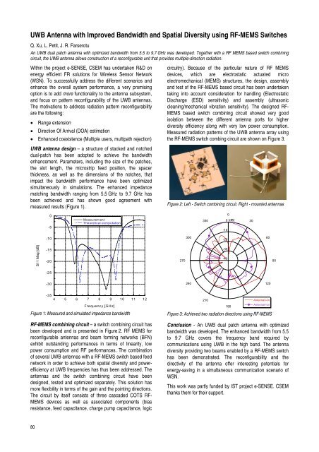
Measured radiation patterns of the UWB antenna array us<strong>in</strong>g<br />
the RF-MEMS switch comb<strong>in</strong>g circuit are shown on Figure 3.<br />
Figure 2: Left - Switch comb<strong>in</strong><strong>in</strong>g circuit. Right - mounted antennas<br />
270<br />
300<br />
240<br />
330<br />
210<br />
0 [dB]<br />
-10<br />
-20<br />
-30<br />
-40<br />
0<br />
180<br />
30<br />
60<br />
120<br />
150Antenna3-on<br />
Antenna4-on<br />
Figure 3: Achieved two radiation directions us<strong>in</strong>g RF-MEMS<br />
Conclusion - An UWB dual patch antenna with optimized<br />
bandwidth was developed. The enhanced bandwidth from 5.5<br />
to 9.7 GHz covers the frequency band required by<br />
communications us<strong>in</strong>g UWB <strong>in</strong> the high band. The antenna<br />
diversity provid<strong>in</strong>g two beams enabled by a RF-MEMS switch<br />
has been demonstrated. The reconfigurability and the<br />
directivity of the antenna offer <strong>in</strong>terest<strong>in</strong>g potentials for<br />
energy-sav<strong>in</strong>g <strong>in</strong> a simultaneous communication scenario of<br />
WSN.<br />
This work was partly funded by IST project e-SENSE. <strong>CSEM</strong><br />
thanks them for their support.<br />
90