research activities in 2007 - CSEM
research activities in 2007 - CSEM
research activities in 2007 - CSEM

Create successful ePaper yourself
Turn your PDF publications into a flip-book with our unique Google optimized e-Paper software.
Nanoporous Membranes for Medical Diagnostics and Drug Discovery<br />
C. Santschi, R. Pug<strong>in</strong>, V. Spassov, S. Berchtold, A. Hoogerwerf<br />
Understand<strong>in</strong>g cellular signal<strong>in</strong>g controlled by cell surface receptors, ion channels and pumps is a key issue of modern biological <strong>research</strong> and drug<br />
development. A platform for high throughput measurements, namely, impedance spectroscopy and fluorescence microscopy, has been developed<br />
and is described below. A nanoporous SiO2/SixNy membrane, where native vesicles can be self-assembled, forms the core of the device. These<br />
membranes comb<strong>in</strong>ed with microfluidic channels are the ma<strong>in</strong> components of the modularly built-up unit.<br />
A rapidly grow<strong>in</strong>g number of molecular targets discovered by<br />
functional genomics and potential therapeutic compounds<br />
produced by chemical synthesis <strong>in</strong>creases the need to<br />
downscale probe formats <strong>in</strong> order to accelerate functional<br />
screen<strong>in</strong>g, and to reduce reagent consumption [1], and costs.<br />
Recent progress <strong>in</strong> micro- and nanotechnology allows the<br />
fabrication of suspended nanoporous SiO2/SixNy membranes<br />
appropriate for screen<strong>in</strong>g transmembrane receptors and<br />
signal<strong>in</strong>g pathways of mammalian cells. In the frame of this<br />
project f<strong>in</strong>anced by CCMX, a versatile platform allow<strong>in</strong>g highthroughput<br />
electrochemical spectroscopy and fluorescence<br />
measurements has been developed. The realization of this<br />
platform is a challeng<strong>in</strong>g task merg<strong>in</strong>g micro, and<br />
nanotechnology. The modularly built platform consists of three<br />
parts: a micro-fluidic component 1), PCB based Si chip-holder<br />
conta<strong>in</strong><strong>in</strong>g SiO2/SixNy membrane 2), and cover 3) (Figure 1).<br />
3)<br />
2)<br />
1)<br />
Figure 1: Schematic draw<strong>in</strong>g of the modular platform with 1) cover 2)<br />
chip-holder 3) micro-fluidic component.<br />
A system of micro-fluidic channels is sealed between two<br />
glass cover slides. The chip-holder is fabricated us<strong>in</strong>g a PCB<br />
board commonly used <strong>in</strong> <strong>in</strong>dustrial electronics. An image of<br />
the chip-holder PCB is displayed <strong>in</strong> Figure 2. The PCB<br />
conta<strong>in</strong>s rectangular apertures, where the <strong>in</strong>dividual silicon<br />
chips are placed. Moreover, electric contacts are directly<br />
<strong>in</strong>tegrated on both sides of the double layered board. The<br />
cover consists of a glass cover slide and a PDMS seal<strong>in</strong>g<br />
layer.<br />
Figure 2: a) Image of the PCB chip-holder with mounted Si chips.<br />
The size of the board is 4 x 10 cm 2 . b) Closed view show<strong>in</strong>g a blank<br />
cutout where the <strong>in</strong>dividual chips can be mounted.<br />
The maximum thickness of the cover is governed by the focal<br />
distance of a fluorescence microscope, which can be as short<br />
54<br />
Glass cover slide<br />
PDMS-Seal<strong>in</strong>g<br />
Chip holder<br />
PDMS-Seal<strong>in</strong>g<br />
Glass cover slide<br />
Fluidic channel<br />
Glass cover slide<br />
Microscope<br />
Fluidic <strong>in</strong>- and<br />
outlets<br />
Si chip (Figure 3)<br />
PDMS<br />
as 350 μm. The micro-fluidic part of the device is sealed<br />
between two glass cover slides.<br />
SiO2 SiN<br />
Pt<br />
Figure 3: Schematic cross-section a Si chip conta<strong>in</strong><strong>in</strong>g a membrane<br />
The SiO2/SixNy membranes are fabricated from a 4 <strong>in</strong>ch silicon<br />
wafer us<strong>in</strong>g standard microfabrication techniques. The wafer<br />
is divided <strong>in</strong>to chips of 5 x 10 mm 2 each conta<strong>in</strong><strong>in</strong>g a<br />
50 x 50 μm 2 freestand<strong>in</strong>g membrane. A schematic crosssection<br />
of the chip is displayed <strong>in</strong> Figure 3. For size selective<br />
position<strong>in</strong>g of the vesicles of <strong>in</strong>terest, each membrane<br />
conta<strong>in</strong>s n<strong>in</strong>e cavities etched <strong>in</strong> the SiO2 layer. Furthermore,<br />
each of the cavities conta<strong>in</strong>s a s<strong>in</strong>gle nanopore of 50 nm <strong>in</strong><br />
diameter <strong>in</strong> the center of the underly<strong>in</strong>g SiN membrane as<br />
illustrated <strong>in</strong> Figure 3. The diameter of the cavities lies <strong>in</strong> the<br />
range of 1 – 2 μm. For prototyp<strong>in</strong>g, cavities and nanopores<br />
have been fabricated us<strong>in</strong>g a Focused Ion Beam (FIB)<br />
technique. FIB is a versatile tool which allows surface<br />
structur<strong>in</strong>g by local material removal. The <strong>in</strong>teraction between<br />
a focused Ga + -beam and the substrate results <strong>in</strong> a physical<br />
removal of material due to a momentum transfer from the<br />
<strong>in</strong>cident ions to the target atoms. Us<strong>in</strong>g FIB, structures of<br />
almost any user-def<strong>in</strong>ed geometry larger than a few tens of<br />
nanometers can be realized; thus, it is an appropriate tool for<br />
the fabrication of nanopores [2] .<br />
500 nm<br />
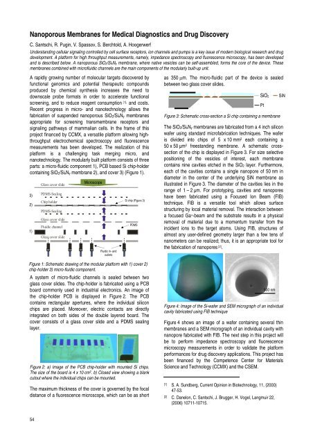
Figure 4: Image of the Si-wafer and SEM micrograph of an <strong>in</strong>dividual<br />
cavity fabricated us<strong>in</strong>g FIB technique<br />
Figure 4 shows an image of a wafer conta<strong>in</strong><strong>in</strong>g several th<strong>in</strong><br />
membranes and a SEM micrograph of an <strong>in</strong>dividual cavity with<br />
nanopore fabricated with FIB. The next step <strong>in</strong> this project will<br />
be to perform impedance spectroscopy and fluorescence<br />
microscopy measurements <strong>in</strong> order to validate the platform<br />
performances for drug discovery applications. This project has<br />
been f<strong>in</strong>anced by the Competence Center for Materials<br />
Science and Technology (CCMX) and the <strong>CSEM</strong>.<br />
[1] S. A. Sundberg, Current Op<strong>in</strong>ion <strong>in</strong> Biotechnology, 11, (2000)<br />
47-53.<br />
[2] C. Danelon, C. Santschi, J. Brugger, H. Vogel, Langmuir 22,<br />
(2006) 10711-10715.