research activities in 2007 - CSEM
research activities in 2007 - CSEM
research activities in 2007 - CSEM

You also want an ePaper? Increase the reach of your titles
YUMPU automatically turns print PDFs into web optimized ePapers that Google loves.
Bond<strong>in</strong>g of Glass or Silicon Chips with a Self-Seal<strong>in</strong>g Photostructurable Elastomer<br />
J. Auerswald, F. Cardot, P. Niedermann, A. Ibzazene, M. Fretz, N. Schmid, H. F. Knapp<br />
When it comes to the <strong>in</strong>tegration of planar electrodes on glass, quartz, silicon or thermoplastic chips <strong>in</strong>to microfluidic systems, standard bond<strong>in</strong>g<br />
methods like diffusion bond<strong>in</strong>g, anodic bond<strong>in</strong>g, thermo-compression bond<strong>in</strong>g etc. do not work. Surfaces carry<strong>in</strong>g electrodes cannot be sealed with<br />
a stiff material. The challenge is even bigger when two glass chips with fac<strong>in</strong>g electrodes and microfluidic channels <strong>in</strong> between are required by the<br />
application, with an alignment precision down to a few micrometers. Photostructurable polysiloxane could be a solution.<br />
The use of photostructurable polysiloxane comb<strong>in</strong>es two<br />
advantages: Firstly, the good alignment precision of<br />
microfluidic channels made by photolithography. Secondly,<br />
the reliable permanent bond of silicones to glass, even if the<br />
glass chips carry electrodes. Photostructurable polysiloxane is<br />
a material known from ISFET and ChemFET sensor<br />
packag<strong>in</strong>g. There, typical lateral structure dimensions are<br />
several millimeters, sometimes slightly below 1 mm, and are<br />
shaped as simple O-r<strong>in</strong>gs [1, 2] . However, the use of this<br />
material class for microfluidic systems with microfluidic<br />
channel networks conta<strong>in</strong><strong>in</strong>g junctions or <strong>in</strong>tersections at<br />
channel widths well below 1 mm, and electrodes <strong>in</strong> the<br />
channels has not been demonstrated yet. One of the critical<br />
issues is the precise bond<strong>in</strong>g of the cured material to the glass<br />
counter chip which also has electrodes on its surface.<br />
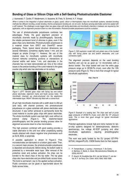
Figure 1: LEFT: Bonded glass chips with fac<strong>in</strong>g top and bottom<br />
planar electrodes, alignment marks and fluidic access holes. The<br />
microfluidic channels are photo-structured <strong>in</strong>to the elastomeric<br />
<strong>in</strong>termediate layer. RIGHT: Bonded chip filled with a colored fluid.<br />
25 μm high microfluidic channels with a width down to 200 μm<br />
(and less), with channel junctions, <strong>in</strong>to photostructured<br />
polysiloxane on a glass substrate with planar electrodes were<br />
structured. It was further achieved to permanently bond the<br />
cured material to counter glass chips with planar electrodes.<br />
The whole microfluidic system was leak tight, even without an<br />
external clamp (Figure 1). The elastomer-based<br />
photolithography and the precise bond<strong>in</strong>g process allow for<br />
alignment accuracies down to a few micrometers.<br />
This high precision comb<strong>in</strong>ed with good seal<strong>in</strong>g provides a<br />
viable alternative to the until now rather unsatisfy<strong>in</strong>g seal<strong>in</strong>g<br />
results obta<strong>in</strong>ed with classic negative tone photoresists such<br />
as SU-8, BCB, or polyimide.<br />
A possible application is shown <strong>in</strong> Figure 2. First,<br />
microelectrodes are fabricated on a bottom glass wafer. Then,<br />
<strong>in</strong> a second mask process, the photostructurable polysiloxane<br />
is deposited and structured. Before dic<strong>in</strong>g, the bottom wafer is<br />
protected by a removable resist layer. After removal of the<br />
protective resist and surface activation, the chips can be<br />
bonded to the diced chips of the top wafer. The top glass<br />
chips also have electrodes and pre-drilled fluidic access holes.<br />
The bond is permanent, due to the applied surface activation.<br />
Fluidic connectors can be glued or tape-bonded above the<br />
fluidic access holes.<br />
Figure 2: CAD explosion model (left) and global view of the bonded<br />
chip with fac<strong>in</strong>g planar top and bottom electrodes, and Luer<br />
connectors (right).<br />
The alignment precision depends on the used bond<strong>in</strong>g<br />
mach<strong>in</strong>e and can be as good as 1-2 micrometers with a<br />
device bonder. The chips sealed well over the entire gage<br />
pressure range up to 28’000 Pa (4 psi), even after the 10th<br />
pressure cycle (Figure 3). This is more than enough for typical<br />
microfluidic applications.<br />
Figure 3: Example of a seal<strong>in</strong>g test. The chips seal well at pump<br />
gage pressures of 30’000 Pa (4 psi), even after the 10 th pressure<br />
cycle. This is more than good enough for typical microfluidic<br />
applications.<br />
Potential applications <strong>in</strong>clude high-end niche markets for labon-chip<br />
systems designed for dielectrophoresis, dielectric<br />
spectroscopy, low voltage AC-EOF pump<strong>in</strong>g and other<br />
microfluidic applications requir<strong>in</strong>g photolithographic<br />
electrodes.<br />
This work was partly funded by the EU (project IST-FP6-<br />
027540, IntegramPLUS). <strong>CSEM</strong> thanks them for their support.<br />
[1] P. Temple-Boyer, J. Launay, I. Humenyuk, T. Do Conto,<br />
A. Mart<strong>in</strong>ez, C. Beriet, A. Grisel, Microelectronics Reliability 44<br />
(2004) 443-447.<br />
[2] P. Arqu<strong>in</strong>t, M. Koudelka-Hep, B.H. van der Schoot, P. van der<br />
Val, N. F. de Rooij, Cl<strong>in</strong>. Chem. 40/9 (1994) 1805-1809.<br />
95