research activities in 2007 - CSEM
research activities in 2007 - CSEM
research activities in 2007 - CSEM

Create successful ePaper yourself
Turn your PDF publications into a flip-book with our unique Google optimized e-Paper software.
A High-Performance 2.4 GHz RF Front-End <strong>in</strong> a 90 nm Process<br />
M. Kucera, N. Scolari, F. Pengg, P. Persech<strong>in</strong>i , D. Ruffieux, A. Vouilloz, E. Vardarli, P. Ferrat, J. Chabloz, R. Caseiro, C. Monneron<br />
The ever ongo<strong>in</strong>g advances <strong>in</strong> semiconductor manufactur<strong>in</strong>g and the cont<strong>in</strong>uous shr<strong>in</strong>k of the <strong>in</strong>tegrated transistors pose new challenges and<br />
require <strong>in</strong>novative solutions for the design of high-performance and low-power RF circuits <strong>in</strong> the ultra-deep submicron range. This paper provides<br />
<strong>in</strong>sight <strong>in</strong> the design of a high performance 2.4 GHz RF front-end <strong>in</strong> 90 nm CMOS.<br />
The well known “Moore’s Law” has been valid for nearly 40<br />
years, confirm<strong>in</strong>g that <strong>in</strong>tegrated circuit (IC) technology<br />
evolves every 18 months with a new process generation that<br />
enables higher circuit <strong>in</strong>tegration and reduced IC size and<br />
cost. While the ma<strong>in</strong> driv<strong>in</strong>g forces are large digital ICs,<br />
analog and RF circuits can also benefit from these technology<br />
advances, <strong>in</strong> particular system-on-chip (SoC) realizations<br />
where they are embedded jo<strong>in</strong>tly with large digital sections<br />
(e.g. mobile telephony ICs).<br />
Concern<strong>in</strong>g radio SoCs, the co-<strong>in</strong>tegration of highperformance<br />
low-power RF circuits together with digital blocks<br />
has been proven us<strong>in</strong>g submicron CMOS<br />
(0.5µm - 0.18µm) [1] . RF-platforms of the next generation,<br />
such as Software Def<strong>in</strong>ed Radios (SDR), rely heavily on large<br />
digital process<strong>in</strong>g blocks [2] , which pleads for us<strong>in</strong>g ultra-deep<br />
submicron (UDSM) CMOS (90 nm and beyond). The<br />
challenge today thus consists of the design of highperformance<br />
RF circuits with competitive sizes of the RF<br />
blocks (UDSM CMOS be<strong>in</strong>g expensive) and with low power<br />
consumption, which is critical for portable, battery operated<br />
applications targeted by <strong>CSEM</strong>.<br />
With<strong>in</strong> this context, <strong>CSEM</strong> has designed a 90 nm CMOS RF<br />
front-end circuit with the follow<strong>in</strong>g goals:<br />
• To achieve high-performance specifications with lowest<br />
possible power consumption while m<strong>in</strong>imiz<strong>in</strong>g the required<br />
silicon area.<br />
• To design <strong>in</strong> a standard digital 90 nm CMOS process,<br />
without rely<strong>in</strong>g on costly RF/analog process<strong>in</strong>g options:<br />
this is mandatory for enabl<strong>in</strong>g seamless co-<strong>in</strong>tegration<br />
with digital circuits.<br />
• To establish a library of optimized RF passive devices: the<br />
generic RF passive devices (<strong>in</strong>ductors, capacitors,<br />
varicaps, etc) provided by silicon foundries usually have<br />
<strong>in</strong>adequate performance and prohibitive sizes, or require<br />
additional process<strong>in</strong>g options. The design of optimized<br />
passives on the standard digital technology is crucial for<br />
achiev<strong>in</strong>g best-<strong>in</strong>-class RF performance.<br />
The RF front-end targets the 2.4 GHz ISM band, and <strong>in</strong>cludes<br />
a receiver front-end (LNA, down-conversion mixers), a<br />
transmitter front-end (PA, up-conversion mixers), and the<br />
critical blocks of the frequency synthesizer (RF VCO, LO<br />
buffers, pre-scalers and multi-modulus dividers). The target<br />
specifications are a noise figure of 2 dB for the receiver frontend<br />
with high l<strong>in</strong>earity (IIP3 up to -13 dBm for an entire<br />
receiver), and a current consumption of 8 mA from a 1.6 V<br />
supply. The transmitter targets +27 dBm of output power<br />
which requires the handl<strong>in</strong>g of about 1 W and 500 mA on-chip.<br />
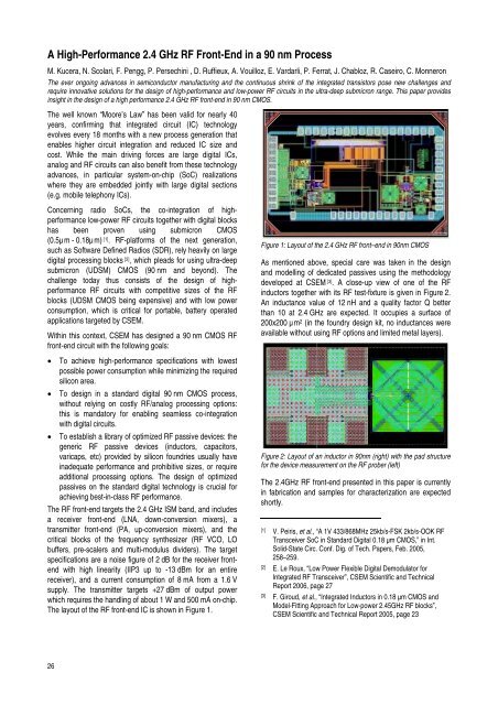
The layout of the RF front-end IC is shown <strong>in</strong> Figure 1.<br />
26<br />
Figure 1: Layout of the 2.4 GHz RF front–end <strong>in</strong> 90nm CMOS<br />
As mentioned above, special care was taken <strong>in</strong> the design<br />
and modell<strong>in</strong>g of dedicated passives us<strong>in</strong>g the methodology<br />
developed at <strong>CSEM</strong> [3] . A close-up view of one of the RF<br />
<strong>in</strong>ductors together with its RF test-fixture is given <strong>in</strong> Figure 2.<br />
An <strong>in</strong>ductance value of 12 nH and a quality factor Q better<br />
than 10 at 2.4 GHz are expected. It occupies a surface of<br />
200x200 µm 2 (<strong>in</strong> the foundry design kit, no <strong>in</strong>ductances were<br />
available without us<strong>in</strong>g RF options and limited metal layers).<br />
Figure 2: Layout of an <strong>in</strong>ductor <strong>in</strong> 90nm (right) with the pad structure<br />
for the device measurement on the RF prober (left)<br />
The 2.4GHz RF front-end presented <strong>in</strong> this paper is currently<br />
<strong>in</strong> fabrication and samples for characterization are expected<br />
shortly.<br />
[1] V. Peiris, et al., “A 1V 433/868MHz 25kb/s-FSK 2kb/s-OOK RF<br />
Transceiver SoC <strong>in</strong> Standard Digital 0.18 μm CMOS,” <strong>in</strong> Int.<br />
Solid-State Circ. Conf. Dig. of Tech. Papers, Feb. 2005,<br />
258–259.<br />
[2] E. Le Roux, “Low Power Flexible Digital Demodulator for<br />
Integrated RF Transceiver”, <strong>CSEM</strong> Scientific and Technical<br />
Report 2006, page 27<br />
[3] F. Giroud, et al., “Integrated Inductors <strong>in</strong> 0.18 μm CMOS and<br />
Model-Fitt<strong>in</strong>g Approach for Low-power 2.45GHz RF blocks”,<br />
<strong>CSEM</strong> Scientific and Technical Report 2005, page 23