research activities in 2007 - CSEM
research activities in 2007 - CSEM
research activities in 2007 - CSEM

Create successful ePaper yourself
Turn your PDF publications into a flip-book with our unique Google optimized e-Paper software.
ArrayFM – An Atomic Force Microscope Us<strong>in</strong>g 2-Dimensional Probe Arrays<br />
A. Meister, J. Polesel-Maris, S. Dasen, G. Gruener, M. Schnieper, T. Overstolz, A. Vuillem<strong>in</strong>, C. Gimkiewicz, R. Ischer, P. Vettiger,<br />
H. He<strong>in</strong>zelmann<br />
In this multidiscipl<strong>in</strong>ary <strong>in</strong>tegrated project, an atomic force microscope able to <strong>in</strong>vestigate large sample surfaces with nanometric resolution was<br />
developed. Instead of a s<strong>in</strong>gle probe, this novel microscope uses a 2-dimensional array of probes operat<strong>in</strong>g <strong>in</strong> parallel. Applications of this<br />
microscope <strong>in</strong>clude the biology doma<strong>in</strong>, quality control, as well as material and surface characterization.<br />
S<strong>in</strong>ce the emergence of the atomic force microscopy (AFM) <strong>in</strong><br />
the eighties, the topographic <strong>in</strong>vestigation of a sample surface<br />
at a nanometric scale has become a standard technique. AFM<br />
techniques can also be used to measure various k<strong>in</strong>ds of local<br />
<strong>in</strong>teractions, such as magnetic, electrostatic, or b<strong>in</strong>d<strong>in</strong>g forces,<br />
electrical conductivity, or to determ<strong>in</strong>e mechanical properties<br />
such as elasticity or friction. Standard AFMs use a s<strong>in</strong>gle<br />
probe, and, due to the scann<strong>in</strong>g process, are rather slow <strong>in</strong><br />
terms of data acquisition. The aim of this project is to develop<br />
an AFM function<strong>in</strong>g with a large probe-array <strong>in</strong>stead of a<br />
s<strong>in</strong>gle probe, <strong>in</strong>creas<strong>in</strong>g thus the throughput of the <strong>in</strong>strument.<br />
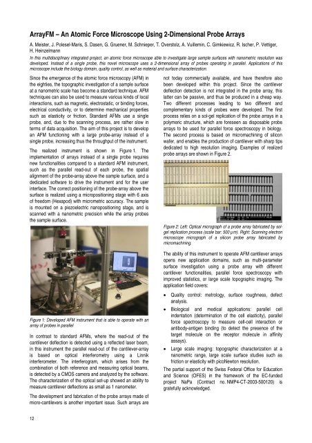
The realized <strong>in</strong>strument is shown <strong>in</strong> Figure 1. The<br />
implementation of arrays <strong>in</strong>stead of a s<strong>in</strong>gle probe requires<br />
new functionalities compared to a standard AFM <strong>in</strong>strument,<br />
such as the parallel read-out of each probe, the spatial<br />
alignment of the probe-array above the sample surface, and a<br />
dedicated software to drive the <strong>in</strong>strument and for the user<br />
<strong>in</strong>terface. The correct position<strong>in</strong>g of the probe-array above the<br />
surface is realized us<strong>in</strong>g a microposition<strong>in</strong>g stage with 6 axis<br />
of freedom (Hexapod) with micrometric accuracy. The sample<br />
is mounted on a piezoelectric nanoposition<strong>in</strong>g stage, and is<br />
scanned with a nanometric precision while the array probes<br />
the sample surface.<br />
Figure 1: Developed AFM <strong>in</strong>strument that is able to operate with an<br />
array of probes <strong>in</strong> parallel<br />
In contrast to standard AFMs, where the read-out of the<br />
cantilever deflection is detected us<strong>in</strong>g a reflected laser beam,<br />
<strong>in</strong> this <strong>in</strong>strument the parallel read-out of the cantilever-array<br />
is based on optical <strong>in</strong>terferometry us<strong>in</strong>g a L<strong>in</strong>nik<br />
<strong>in</strong>terferometer. The <strong>in</strong>terferogram, which arises from the<br />
comb<strong>in</strong>ation of both reference and measur<strong>in</strong>g optical beams,<br />
is detected by a CMOS camera and analyzed by the software.<br />
The characterization of the optical set-up showed an ability to<br />
measure cantilever deflections as small as 1 nanometer.<br />
The development and fabrication of the probe arrays made of<br />
micro-cantilevers is another important issue. Such arrays are<br />
12<br />
not today commercially available, and have therefore also<br />
been developed with<strong>in</strong> this project. S<strong>in</strong>ce the cantilever<br />
deflection detection is not <strong>in</strong>tegrated <strong>in</strong> the probe array, this<br />
latter can be passive, and thus be produced <strong>in</strong> a cheap way.<br />
Two different processes lead<strong>in</strong>g to two different and<br />
complementary k<strong>in</strong>ds of probes were developed. The first<br />
process relies on a sol-gel replication of the probe arrays <strong>in</strong> a<br />
polymeric structure, which are foreseen as disposable probe<br />
arrays to be used for parallel force spectroscopy <strong>in</strong> biology.<br />
The second process is based on micromach<strong>in</strong><strong>in</strong>g of silicon<br />
wafer, and enables the production of cantilever with sharp tips<br />
dedicated to high resolution imag<strong>in</strong>g. Examples of realized<br />
probe arrays are shown <strong>in</strong> Figure 2.<br />
Figure 2: Left: Optical micrograph of a probe array fabricated by solgel<br />
replication process (scale bar: 500 µm). Right: Scann<strong>in</strong>g electron<br />
microscope micrograph of a silicon probe array fabricated by<br />
micromach<strong>in</strong><strong>in</strong>g.<br />
The ability of this <strong>in</strong>strument to operate AFM cantilever arrays<br />
opens new application doma<strong>in</strong>s, such as multi-parameter<br />
surface <strong>in</strong>vestigation us<strong>in</strong>g a probe array with different<br />
cantilever functionalities, parallel force spectroscopy with<br />
improved statistics, or large scale topographic imag<strong>in</strong>g. The<br />
application field covers:<br />
• Quality control: metrology, surface roughness, defect<br />
analysis.<br />
• Biological and medical applications: parallel cell<br />
<strong>in</strong>dentation (determ<strong>in</strong>ation of the cell elasticity), parallel<br />
force spectroscopy to measure cell-cell <strong>in</strong>teraction or<br />
antibody-antigen b<strong>in</strong>d<strong>in</strong>g (to detect the presence of the<br />
target molecule on the receptor molecule <strong>in</strong> aff<strong>in</strong>ity<br />
assays).<br />
• Large scale imag<strong>in</strong>g: topographic characterization at a<br />
nanometric range, large scale surface studies such as<br />
friction or elasticity with picoNewton resolution.<br />
The partial support of the Swiss Federal Office for Education<br />
and Science (OFES) <strong>in</strong> the framework of the EC-funded<br />
project NaPa (Contract no. NMP4-CT-2003-500120) is<br />
gratefully acknowledged.