

Logic selection guide 2016
1Sk34oD
1Sk34oD

You also want an ePaper? Increase the reach of your titles
YUMPU automatically turns print PDFs into web optimized ePapers that Google loves.
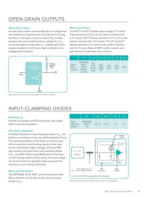
OPEN-DRAIN OUTPUTS<br />
Open-drain outputs<br />
An open-drain output can be pulled up to a voltage level<br />
that matches the requirements of the device it’s driving.<br />
As shown in the figure, a pull-up resistor (R PU<br />
) is used<br />
between the output and the pull-up voltage (V PU<br />
). V PU<br />
can be set higher or lower than V CC<br />
, making open-drain<br />
outputs suitable for both low-to-high and high-to-low<br />
voltage-level translation.<br />
Where you’ll find it<br />
The AHCT and HCT families support legacy TTL levels.<br />
They operate at 5 V and can be used to interface with<br />
3.3 V inputs. AUP1T devices operate at 3.3 V and can be<br />
used to interface with 1.8 V inputs. The LVT and ALVT<br />
families operate at 3.3 V and can be used to interface<br />
with 2.5 V inputs. Many of NXP’s buffer, inverter, and<br />
gate devices include open-drain outputs.<br />
V PU<br />
5 V 3.3 V 2.5 V 1.8 V 1.2 V 0.8 V<br />
Input<br />
Level shifter<br />
with open-drain<br />
output<br />
Pull-up<br />
resistor<br />
(R PU<br />
)<br />
Opendrain<br />
outputs<br />
HEF4000B,<br />
NPIC,<br />
HC(T),<br />
AHC(T),<br />
LV, LVC<br />
HC,<br />
AHC,<br />
LV, LVC,<br />
AUP<br />
LVC,<br />
AUP,<br />
AXP<br />
AUP,<br />
AXP<br />
AUP,<br />
AXP<br />
AXP<br />
GND<br />
Open-drain output and pull-up resistor for level translation<br />
INPUT-CLAMPING DIODES<br />
What they do<br />
Provide overvoltage and ESD protection, and enable<br />
high-to-low level translation.<br />
Inputclamping<br />
diodes<br />
5 V 3.3 V 2.5 V 1.8 V 1.2 V<br />
HEF4000B,<br />
HC(T),<br />
LV<br />
HC, LV HC, LV LV LV<br />
Why they’re important<br />
In families that have an input-clamping diode to V CC<br />
, the<br />
diode is a critical part of the input ESD-protection circuit.<br />
Clamping<br />
diode<br />
The clamping property of the diode can also be used<br />
with an external current-limiting resistor so the input<br />
V CC2 = 5 V<br />
can be interfaced to higher voltages. On some NXP<br />
logic devices, the inputs have input-clamping diodes<br />
V CC1<br />
= 15 V<br />
to V CC<br />
and GND. When using CMOS devices that have<br />
Device A<br />
current-limiting resistors at the inputs, the input voltage<br />
can exceed maximum specified values as long as the<br />
maximum current rating is observed.<br />
R CL<br />
GND<br />
Where you’ll find them<br />
The HEF4000B, HC(T), NPIC, and LV families all utilize<br />
ESD-protection circuits that include input-clamping<br />
diodes to V CC<br />
.<br />
R CL<br />
=<br />
15 V - (5.0 V + 0.7 V)<br />
I IK<br />
ESD<br />
protection<br />
I IK<br />
is found in the limiting values table of the datasheet<br />
Input<br />
buffer<br />
Input-clamping diodes support high-to-low level translation<br />
NXP <strong>Logic</strong> <strong>selection</strong> <strong>guide</strong> <strong>2016</strong><br />
23