Physical Principles of Electron Microscopy: An Introduction to TEM ...
Physical Principles of Electron Microscopy: An Introduction to TEM ...
Physical Principles of Electron Microscopy: An Introduction to TEM ...

Create successful ePaper yourself
Turn your PDF publications into a flip-book with our unique Google optimized e-Paper software.
<strong>TEM</strong> Specimens and Images 123<br />
<strong>of</strong> a semiconduc<strong>to</strong>r material. This instrument also gives an electron or ionbeam<br />
image <strong>of</strong> the surface <strong>of</strong> the specimen, allowing the ion beam <strong>to</strong> be<br />
positioned and scanned along a line in order <strong>to</strong> cut a slice <strong>of</strong> material at a<br />
precise location. In this way, it is possible <strong>to</strong> prepare a <strong>TEM</strong> specimen that<br />
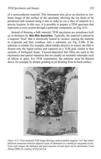
represents a cross section through a particular component; see Fig. 4-21.<br />
Instead <strong>of</strong> thinning a bulk material, <strong>TEM</strong> specimens are sometimes built<br />
up in thickness by thin-film deposition. Typically, the material is placed in<br />
a tungsten “boat” that is electrically heated in vacuum, causing the material<br />
<strong>to</strong> evaporate and then condense on<strong>to</strong> a substrate; see Fig. 4.20h. If the<br />
substrate is soluble (for example, alkali halides dissolve in water), the film is<br />
floated on<strong>to</strong> the liquid surface and captured on a <strong>TEM</strong> grid, similar <strong>to</strong> thin<br />
sections <strong>of</strong> biological tissue. Vacuum-deposited thin films are used in the<br />
electronics and optical industries but are usually on insoluble substrates such<br />
as silicon or glass. For <strong>TEM</strong> examination, the substrate must be thinned<br />
down, for example by dimple grinding or jet thinning from its back surface.<br />
Figure 4-21. Cross-sectional <strong>TEM</strong> image showing a polycrystalline tungsten “via” that makes<br />
electrical connection between adjacent layers <strong>of</strong> aluminum in a multilayer integrated circuit.<br />
From such images, the thickness and grain structure <strong>of</strong> each layer can be determined. From<br />
Zhang (2000), by courtesy <strong>of</strong> Elsevier Ltd.