PXA3xx Boot ROM Reference Manual - Marvell
PXA3xx Boot ROM Reference Manual - Marvell
PXA3xx Boot ROM Reference Manual - Marvell
- No tags were found...
You also want an ePaper? Increase the reach of your titles
YUMPU automatically turns print PDFs into web optimized ePapers that Google loves.
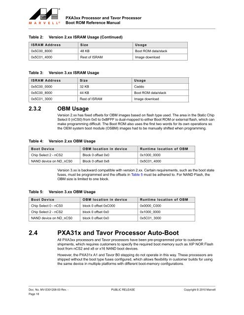
<strong>PXA3xx</strong> Processor and Tavor Processor<strong>Boot</strong> <strong>ROM</strong> <strong>Reference</strong> <strong>Manual</strong>Table 2:Version 2.xx ISRAM Usage (Continued)ISRAM Address Size Usage0x5C00_8000 48 KB <strong>Boot</strong> <strong>ROM</strong> data/stack0x5C01_4000 Rest of ISRAM Image downloadTable 3:Version 3.xx ISRAM UsageISRAM Address Size Usage0x5C00_0000 32 KB Caddo0x5C00_8000 44 KB <strong>Boot</strong> <strong>ROM</strong> data/stack0x5C01_3000 Rest of ISRAM Image download2.3.2 OBM UsageVersion 2.xx has fixed offsets for OBM images based on flash type used. The area in the Static ChipSelect 0 (nCS0) from 0x0 to 0xBFFF is dual-mapped to either <strong>Boot</strong> <strong>ROM</strong> or external flash, which canmake programming difficult. The <strong>Boot</strong> <strong>ROM</strong> also uses the first two words for its own operations sothe OEM system boot module (OSBM) images had to be manually shifted when programming.Table 4:Version 2.xx OBM Usage<strong>Boot</strong> Device OBM location in device Runtime location of OBMChip Select 2 - nCS2 Block 0 offset 0x0 0x1000_0000NAND device on ND_nCS0 Block 0 offset 0x8 0x5C01_4000Version 3.xx is backward compatible with version 2.xx. Certain requirements, such as the boot statefuses, must be programmed and the offsets in Table 5 must be adhered to. For NAND Flash, theOBM size is limited to one block.Table 5:Version 3.xx OBM Usage<strong>Boot</strong> Device OBM location in device Runtime location of OBMChip Select 0 - nCS0 block 0 offset 0xC000 0x0000_C000Chip Select 2 - nCS2 block 0 offset 0x0 0x1000_0000NAND device on ND_nCS0 block 0 offset 0x0 0x5C01_30002.4 PXA31x and Tavor Processor Auto-<strong>Boot</strong>All <strong>PXA3xx</strong> processors and Tavor processors have been pre-programmed prior to customershipments, which requires customers to specify the required boot memory such as XIP NOR Flashboot from nCS2 and x8 or x16 NAND boot devices.However, the PXA31x A1 and Tavor B0 stepping do not operate in this way. These processors areshipped without the boot type fuses configured, which allows flexibility in customer builds for usingthe same device in multiple platforms with different boot-memory configurations.Doc. No. MV-S301208-00 Rev. - PUBLIC RELEASE Copyright © 2010 <strong>Marvell</strong>Page 18


