PXA3xx Boot ROM Reference Manual - Marvell
PXA3xx Boot ROM Reference Manual - Marvell
PXA3xx Boot ROM Reference Manual - Marvell
- No tags were found...
Create successful ePaper yourself
Turn your PDF publications into a flip-book with our unique Google optimized e-Paper software.
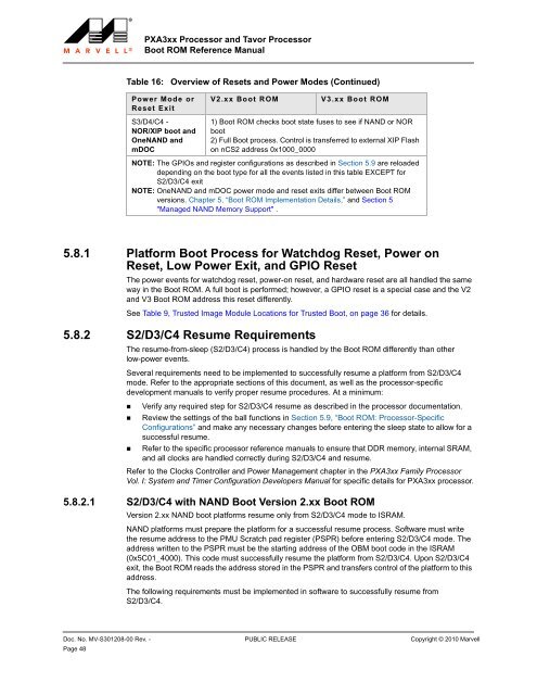
<strong>PXA3xx</strong> Processor and Tavor Processor<strong>Boot</strong> <strong>ROM</strong> <strong>Reference</strong> <strong>Manual</strong>Table 16:Power Mode orReset ExitS3/D4/C4 -NOR/XIP boot andOneNAND andmDOCOverview of Resets and Power Modes (Continued)V2.xx <strong>Boot</strong> <strong>ROM</strong>5.8.1 Platform <strong>Boot</strong> Process for Watchdog Reset, Power onReset, Low Power Exit, and GPIO ResetThe power events for watchdog reset, power-on reset, and hardware reset are all handled the sameway in the <strong>Boot</strong> <strong>ROM</strong>. A full boot is performed; however, a GPIO reset is a special case and the V2and V3 <strong>Boot</strong> <strong>ROM</strong> address this reset differently.See Table 9, Trusted Image Module Locations for Trusted <strong>Boot</strong>, on page 36 for details.5.8.2 S2/D3/C4 Resume RequirementsV3.xx <strong>Boot</strong> <strong>ROM</strong>1) <strong>Boot</strong> <strong>ROM</strong> checks boot state fuses to see if NAND or NORboot2) Full <strong>Boot</strong> process. Control is transferred to external XIP Flashon nCS2 address 0x1000_0000NOTE: The GPIOs and register configurations as described in Section 5.9 are reloadeddepending on the boot type for all the events listed in this table EXCEPT forS2/D3/C4 exitNOTE: OneNAND and mDOC power mode and reset exits differ between <strong>Boot</strong> <strong>ROM</strong>versions. Chapter 5, “<strong>Boot</strong> <strong>ROM</strong> Implementation Details,” and Section 5"Managed NAND Memory Support" .The resume-from-sleep (S2/D3/C4) process is handled by the <strong>Boot</strong> <strong>ROM</strong> differently than otherlow-power events.Several requirements need to be implemented to successfully resume a platform from S2/D3/C4mode. Refer to the appropriate sections of this document, as well as the processor-specificdevelopment manuals to verify proper resume procedures. At a minimum:• Verify any required step for S2/D3/C4 resume as described in the processor documentation.• Review the settings of the ball functions in Section 5.9, “<strong>Boot</strong> <strong>ROM</strong>: Processor-SpecificConfigurations” and make any necessary changes before entering the sleep state to allow for asuccessful resume.• Refer to the specific processor reference manuals to ensure that DDR memory, internal SRAM,and all clocks are handled correctly during S2/D3/C4 and resume.Refer to the Clocks Controller and Power Management chapter in the <strong>PXA3xx</strong> Family ProcessorVol. I: System and Timer Configuration Developers <strong>Manual</strong> for specific details for <strong>PXA3xx</strong> processor.5.8.2.1 S2/D3/C4 with NAND <strong>Boot</strong> Version 2.xx <strong>Boot</strong> <strong>ROM</strong>Version 2.xx NAND boot platforms resume only from S2/D3/C4 mode to ISRAM.NAND platforms must prepare the platform for a successful resume process. Software must writethe resume address to the PMU Scratch pad register (PSPR) before entering S2/D3/C4 mode. Theaddress written to the PSPR must be the starting address of the OBM boot code in the ISRAM(0x5C01_4000). This code must successfully resume the platform from S2/D3/C4. Upon S2/D3/C4exit, the <strong>Boot</strong> <strong>ROM</strong> reads the address stored in the PSPR and transfers control of the platform to thisaddress.The following requirements must be implemented in software to successfully resume fromS2/D3/C4.12345678910111213141516171819202122232425262728293031323334353637383940414243444546474849505152535455565758Doc. No. MV-S301208-00 Rev. - PUBLIC RELEASE Copyright © 2010 <strong>Marvell</strong>Page 48


