PXA3xx Boot ROM Reference Manual - Marvell
PXA3xx Boot ROM Reference Manual - Marvell
PXA3xx Boot ROM Reference Manual - Marvell
- No tags were found...
You also want an ePaper? Increase the reach of your titles
YUMPU automatically turns print PDFs into web optimized ePapers that Google loves.
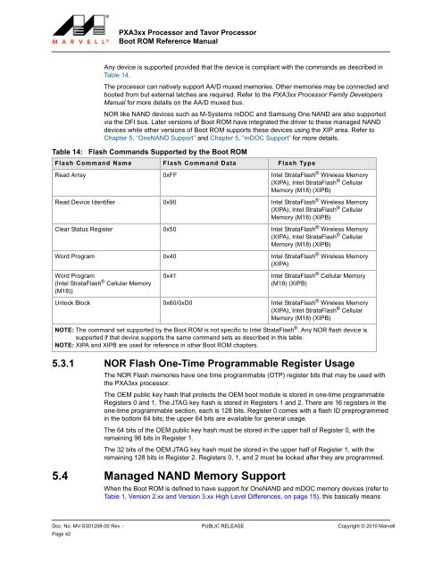
<strong>PXA3xx</strong> Processor and Tavor Processor<strong>Boot</strong> <strong>ROM</strong> <strong>Reference</strong> <strong>Manual</strong>Table 14:Any device is supported provided that the device is compliant with the commands as described inTable 14.The processor can natively support AA/D muxed memories. Other memories may be connected andbooted from but external latches are required. Refer to the <strong>PXA3xx</strong> Processor Family Developers<strong>Manual</strong> for more details on the AA/D muxed bus.NOR like NAND devices such as M-Systems mDOC and Samsung One NAND are also supportedvia the DFI bus. Later versions of <strong>Boot</strong> <strong>ROM</strong> have integrated the driver to these managed NANDdevices while other versions of <strong>Boot</strong> <strong>ROM</strong> supports these devices using the XIP area. Refer toChapter 5, “OneNAND Support” and Chapter 5, “mDOC Support” for more details.Flash Commands Supported by the <strong>Boot</strong> <strong>ROM</strong>Flash Command Name Flash Command Data Flash TypeRead Array 0xFF Intel StrataFlash ® Wireless Memory(XIPA), Intel StrataFlash ® CellularMemory (M18) (XIPB)Read Device Identifier 0x90 Intel StrataFlash ® Wireless Memory(XIPA), Intel StrataFlash ® CellularMemory (M18) (XIPB)Clear Status Register 0x50 Intel StrataFlash ® Wireless Memory(XIPA), Intel StrataFlash ® CellularMemory (M18) (XIPB)Word Program 0x40 Intel StrataFlash ® Wireless Memory(XIPA)Word Program(Intel StrataFlash ® Cellular Memory(M18))0x415.3.1 NOR Flash One-Time Programmable Register UsageThe NOR Flash memories have one time programmable (OTP) register bits that may be used withthe <strong>PXA3xx</strong> processor.The OEM public key hash that protects the OEM boot module is stored in one-time programmableRegisters 0 and 1. The JTAG key hash is stored in Registers 1 and 2. There are 16 registers in theone-time programmable section, each is 128 bits. Register 0 comes with a flash ID preprogrammedin the bottom 64 bits; the upper 64 bits are available for general usage.The 64 bits of the OEM public key hash must be stored in the upper half of Register 0, with theremaining 96 bits in Register 1.The 32 bits of the OEM JTAG key hash must be stored in the upper half of Register 1, with theremaining 128 bits in Register 2. Registers 0, 1, and 2 must be locked after they are programmed.5.4 Managed NAND Memory SupportIntel StrataFlash ® Cellular Memory(M18) (XIPB)Unlock Block 0x60/0xD0 Intel StrataFlash ® Wireless Memory(XIPA), Intel StrataFlash ® CellularMemory (M18) (XIPB)NOTE: The command set supported by the <strong>Boot</strong> <strong>ROM</strong> is not specific to Intel StrataFlash ® . Any NOR flash device issupported if that device supports the same command sets as described in this table.NOTE: XIPA and XIPB are used for reference in other <strong>Boot</strong> <strong>ROM</strong> chapters.When the <strong>Boot</strong> <strong>ROM</strong> is defined to have support for OneNAND and mDOC memory devices (refer toTable 1, Version 2.xx and Version 3.xx High Level Differences, on page 15), this basically means12345678910111213141516171819202122232425262728293031323334353637383940414243444546474849505152535455565758Doc. No. MV-S301208-00 Rev. - PUBLIC RELEASE Copyright © 2010 <strong>Marvell</strong>Page 42


