PXA3xx Boot ROM Reference Manual - Marvell
PXA3xx Boot ROM Reference Manual - Marvell
PXA3xx Boot ROM Reference Manual - Marvell
- No tags were found...
Create successful ePaper yourself
Turn your PDF publications into a flip-book with our unique Google optimized e-Paper software.
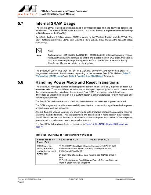
<strong>PXA3xx</strong> Processor and Tavor Processor<strong>Boot</strong> <strong>ROM</strong> <strong>Reference</strong> <strong>Manual</strong>5.7 Internal SRAM UsageThe internal SRAM is used as a data area and to download images from the download ports or theNAND flash. The internal SRAM starts at 0x5c00_0000 and the end is implementation defined (upto 768KBytes max for PXA32x).By default, the lower 32KB of internal SRAM is locked by the Wireless Trusted Module (WTM). The<strong>Boot</strong> <strong>ROM</strong> unlocks 31KB of SRAM from 0x5c00_0400 to 0x5c00_8000 and uses the space to set upstack usage.NoteNoteSoftware must NOT disable the D0CKEN_B[17] bit prior to entering low power modes.Although this bit allows software to enable and disable the Mini-LCD clock, this clock isalso used internally during this sequence. Refer to the <strong>PXA3xx</strong> Processor FamilyDevelopers <strong>Manual</strong> for details on clock gating.The <strong>Boot</strong> <strong>ROM</strong> uses 44 KB (ver 3.xx) or 48 KB (ver 2.xx) above the 32KB for the data area. Allimage downloads are to the addresses, depending on the version of <strong>Boot</strong> <strong>ROM</strong>. Refer to Table 3,“Version 3.xx ISRAM Usage" and Table 4, “Version 2.xx OBM Usage" for details.5.8 Handling Power Mode and Reset TransitionsThe <strong>Boot</strong> <strong>ROM</strong> manages the task of booting up the system which is not only at power-on-reset butalso reset exits. There are differences that must be managed, depending on the mode or reset statethat is being entered or exited and the version of <strong>Boot</strong> <strong>ROM</strong>. This section establishes thosedifferences so that implementation into a system design is better understood for both hardware andsoftware perspectives.The <strong>Boot</strong> <strong>ROM</strong> performs the basic checks to determine the last reset exit or power mode exit.The OBM image must be able to successfully transition the processor through the entire low poweror reset, entry, and exit sequence.Any exit from the various resets or low power mode exits, including booting the processor, requiressteps that must be followed. These requirements are documented in more detail in the processorspecificdeveloper manuals. <strong>Marvell</strong> recommends that these chapters be consulted to ensure propersystem reset procedures and low power modes resumes.The <strong>Boot</strong> <strong>ROM</strong> follows basic tasks as described in Table 15, OneNAND Device ID Support, onpage 44.Table 16:Power Mode orReset ExitPOR (power onreset), Hardwareand Watchdog resetNAND bootOverview of Resets and Power ModesV2.xx <strong>Boot</strong> <strong>ROM</strong>V3.xx <strong>Boot</strong> <strong>ROM</strong>1) ARSR[HWR] and [WDG] is read to ensure that POR/HWRreset has occurred. NOTE: This step only occurs for thePXA32x and PXA30x A12) <strong>Boot</strong> <strong>ROM</strong> checks boot state fuses to see if NAND or NORboot3) Full <strong>Boot</strong> process. ReadID issued from NFC to NAND device.OBM in Block 0 copied to iSRAM.12345678910111213141516171819202122232425262728293031323334353637383940414243444546474849505152535455565758Doc. No. MV-S301208-00 Rev. - PUBLIC RELEASE Copyright © 2010 <strong>Marvell</strong>Page 46


