Heiss W.D. (ed.) Quantum dots.. a doorway to - tiera.ru
Heiss W.D. (ed.) Quantum dots.. a doorway to - tiera.ru
Heiss W.D. (ed.) Quantum dots.. a doorway to - tiera.ru

Create successful ePaper yourself
Turn your PDF publications into a flip-book with our unique Google optimized e-Paper software.
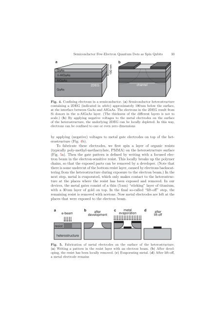
GaAs<br />
n-AlGaAs<br />
AlGaAs<br />
GaAs<br />
Semiconduc<strong>to</strong>r Few-Electron <strong>Quantum</strong> Dots as Spin Qubits 33<br />
a b<br />
2DEG<br />
100 nm<br />
channel<br />
Fig. 4. Confining electrons in a semiconduc<strong>to</strong>r. (a) Semiconduc<strong>to</strong>r heterost<strong>ru</strong>cture<br />
containing a 2DEG (indicat<strong>ed</strong> in white) approximately 100 nm below the surface,<br />
at the interface between GaAs and AlGaAs. The electrons in the 2DEG result from<br />
Si donors in the n-AlGaAs layer. (The thickness of the different layers is not <strong>to</strong><br />
scale.) (b) By applying negative voltages <strong>to</strong> the metal electrodes on the surface<br />
of the heterost<strong>ru</strong>cture, the underlying 2DEG can be locally deplet<strong>ed</strong>. In this way,<br />
electrons can be confin<strong>ed</strong> <strong>to</strong> one or even zero dimensions<br />
by applying (negative) voltages <strong>to</strong> metal gate electrodes on <strong>to</strong>p of the heterost<strong>ru</strong>cture<br />
(Fig. 4b).<br />
To fabricate these electrodes, we first spin a layer of organic resists<br />
(typically poly-methyl-methacrylate, PMMA) on the heterost<strong>ru</strong>cture surface<br />
(Fig. 5a). Then the gate pattern is defin<strong>ed</strong> by writing with a focus<strong>ed</strong> electron<br />
beam in the electron-sensitive resist. This locally breaks up the polymer<br />
chains, so that the expos<strong>ed</strong> parts can be remov<strong>ed</strong> by a developer. (Note that<br />
there is some undercut of the bot<strong>to</strong>m resist layer, caus<strong>ed</strong> by electrons backscattering<br />
from the heterost<strong>ru</strong>cture during exposure <strong>to</strong> the electron beam.) In the<br />
next step, metal is evaporat<strong>ed</strong>, which only makes contact <strong>to</strong> the heterost<strong>ru</strong>cture<br />
at the places where the resist has been expos<strong>ed</strong> and remov<strong>ed</strong>. In our<br />
devices, the metal gates consist of a thin (5 nm) “sticking” layer of titanium,<br />
with a 30 nm layer of gold on <strong>to</strong>p. In the final so-call<strong>ed</strong> “lift-off” step, the<br />
remaining resist is remov<strong>ed</strong> with ace<strong>to</strong>ne. Now metal electrodes are left at the<br />
places that were expos<strong>ed</strong> <strong>to</strong> the electron beam.<br />
a b<br />
e-beam<br />
after c metal d<br />
evaporation<br />
development<br />
resist<br />
heterost<strong>ru</strong>cture<br />
after<br />
lift-off<br />
Fig. 5. Fabrication of metal electrodes on the surface of the heterost<strong>ru</strong>cture.<br />
(a) Writing a pattern in the resist layer with an electron beam. (b) After developing,<br />
the resist has been locally remov<strong>ed</strong>. (c) Evaporating metal. (d) After lift-off,<br />
a metal electrode remains