Heiss W.D. (ed.) Quantum dots.. a doorway to - tiera.ru
Heiss W.D. (ed.) Quantum dots.. a doorway to - tiera.ru
Heiss W.D. (ed.) Quantum dots.. a doorway to - tiera.ru

Create successful ePaper yourself
Turn your PDF publications into a flip-book with our unique Google optimized e-Paper software.
B //<br />
Semiconduc<strong>to</strong>r Few-Electron <strong>Quantum</strong> Dots as Spin Qubits 61<br />
a b<br />
T<br />
DRAIN<br />
RESERVOIR<br />
200 nm M P R<br />
IQPC<br />
Q<br />
SOURCE<br />
c<br />
d<br />
0<br />
-V P<br />
∆I QPC<br />
E F<br />
Γ<br />
τ τ<br />
Γ<br />
time<br />
time<br />
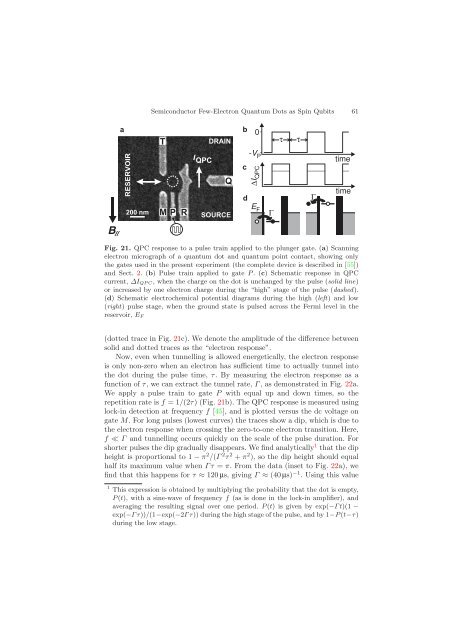
Fig. 21. QPC response <strong>to</strong> a pulse train appli<strong>ed</strong> <strong>to</strong> the plunger gate. (a) Scanning<br />
electron micrograph of a quantum dot and quantum point contact, showing only<br />
the gates us<strong>ed</strong> in the present experiment (the complete device is describ<strong>ed</strong> in [55])<br />
and Sect. 2. (b) Pulse train appli<strong>ed</strong> <strong>to</strong> gate P .(c) Schematic response in QPC<br />
current, ∆IQP C, when the charge on the dot is unchang<strong>ed</strong> by the pulse (solid line)<br />
or increas<strong>ed</strong> by one electron charge during the “high” stage of the pulse (dash<strong>ed</strong>).<br />
(d) Schematic electrochemical potential diagrams during the high (left) andlow<br />
(right) pulse stage, when the ground state is puls<strong>ed</strong> across the Fermi level in the<br />
reservoir, EF<br />
(dott<strong>ed</strong> trace in Fig. 21c). We denote the amplitude of the difference between<br />
solid and dott<strong>ed</strong> traces as the “electron response”.<br />
Now, even when tunnelling is allow<strong>ed</strong> energetically, the electron response<br />
is only non-zero when an electron has sufficient time <strong>to</strong> actually tunnel in<strong>to</strong><br />
the dot during the pulse time, τ. By measuring the electron response as a<br />
function of τ, we can extract the tunnel rate, Γ , as demonstrat<strong>ed</strong> in Fig. 22a.<br />
We apply a pulse train <strong>to</strong> gate P with equal up and down times, so the<br />
repetition rate is f =1/(2τ) (Fig. 21b). The QPC response is measur<strong>ed</strong> using<br />
lock-in detection at frequency f [45], and is plott<strong>ed</strong> versus the dc voltage on<br />
gate M. For long pulses (lowest curves) the traces show a dip, which is due <strong>to</strong><br />
the electron response when crossing the zero-<strong>to</strong>-one electron transition. Here,<br />
f ≪ Γ and tunnelling occurs quickly on the scale of the pulse duration. For<br />
shorter pulses the dip gradually disappears. We find analytically 1 that the dip<br />
height is proportional <strong>to</strong> 1 − π 2 /(Γ 2 τ 2 + π 2 ), so the dip height should equal<br />
half its maximum value when Γτ = π. From the data (inset <strong>to</strong> Fig. 22a), we<br />
find that this happens for τ ≈ 120 µs, giving Γ ≈ (40 µs) −1 . Using this value<br />
1 This expression is obtain<strong>ed</strong> by multiplying the probability that the dot is empty,<br />
P (t), with a sine-wave of frequency f (as is done in the lock-in amplifier), and<br />
averaging the resulting signal over one period. P (t) is given by exp(−Γt)(1 −<br />
exp(−Γτ))/(1−exp(−2Γτ)) during the high stage of the pulse, and by 1−P (t−τ)<br />
during the low stage.